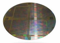
Wafer-scale imager targets medical imaging applications
Engineers at the Science and Technology Facilities Council’s (STFC; Didcot, UK) Rutherford Appleton Laboratory (RAL) have designed a wafer-scale digital image sensor for mammography and digital tomosynthesis applications.
Measuring 120 x 145 mm and effectively using an entire 200 mm silicon wafer in its production, the image sensor was designed using tools from Tanner EDA (Monrovia, CA, USA), and is being manufactured by TowerJazz (Migdal Haemek, Israel), a specialty CMOS semiconductor foundry.
Traditionally, CMOS imagers have the required electronic circuitry implemented on two sides of an imaging array to address the individual sensor pixels. However, the STFC CMOS sensor design group developed electronic circuitry to implement the necessary pixel readout and row-addressing driver functions on just one edge of each sensor, with extra circuitry embedded in the actual pixel array.
This allows multiple sensors, manufactured on 200 mm silicon wafers, to be 'butted' or 'tiled' together to form a significantly larger imaging area and to meet the requirements for medical applications.
The sensor has 6.7-million (2800 x 2400) pixels on a 50-micron pitch, 32 analog outputs and a programmable region-of-interest readout. A clocking scheme called pixel binning is used to combine the charge collected by several adjacent pixels, and is designed to reduce noise and improve the signal-to-noise ratio and frame rate, allowing the sensor to operate at 40 frames/sec at full resolution.
Dr. Renato Turchetta from the Rutherford Appleton Laboratory will be giving a presentation on the CMOS image sensor at the CMOS Emerging Technologies conference (Vancouver, Canada) from July 18-21, 2012.
-- by Dave Wilson, Senior Editor, Vision Systems Design
