AUTOMOTIVE MANUFACTURING: Vision sensors error-proof oil cap assembly
Miniature Precision Components (MPC; Prairie du Chien, WI, USA;www.mpc-inc.com) is using three vision sensors from Cognex (Natick, MA, USA; www.cognex.com) to error-proof the automated assembly of oil caps. MPC’s oil-cap assembly system installs o-ring seals into molded thermoplastic caps and then prints on top of the caps. The system uses two vibratory bowl feeders, one to feed o-rings and the other to feed oil caps into the assembly process. As the bowls vibrate, the parts move up a spiral ramp on the side of the feeders to an inline conveyor.
At the end of the inline conveyor, a pick-and-place arm transfers o-rings to the first station on a rotary assembly dial. After an o-ring is loaded onto the dial fixture, it indexes to the second station. There, another inline conveyor feeds blank caps to a second pick-and-place arm that presses the caps on top of the loaded seals. Then the assembled cap and seal continue through the pad printing and final inspection stations.
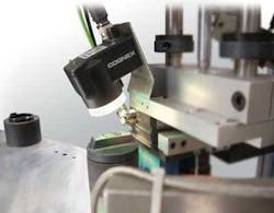
Tight control of o-ring and cap orientation is critical to ensure the seal is properly installed so that the finished oil cap will function as intended. The cap must also be in the proper orientation prior to pad printing. Because the hard tooling and traditional sensors in the cap assembly system proved unreliable, MPC selected three Checker 202 vision sensors to ensure proper o-ring and cap orientation (see figure).
While the first sensor detects inverted o-rings between the vibratory feeder bowl and inline conveyor, a second vision sensor checks that the o-ring is positioned properly on the dial fixture before the cap is pressed on. Lastly, proper cap orientation is determined by a third sensor prior to assembly and printing.
Each o-ring has a sealing bead on one side. This bead must be placed facedown when the seal is loaded; otherwise, the machine shuts down. The operator must then access and reposition the seal before restarting the machine. Although mechanical tooling on the feeder bowl was designed to prevent inverted o-rings from entering the process, the tooling was unreliable and slightly warped or not perfectly flat o-rings were occasionally loaded upside down, causing the machine to shut down.
“Having the operator flip these seals and restart the machine was reducing production efficiency,” says Shane Harsha, MPC’s manufacturing engineering manager. “If the production rate dropped from 360 to 200 caps per hour, it cost us about $20,000 a year in downtime. As we approach full production volumes, that cost could increase to as much as $120,000 per year.”
To detect the inverted o-rings in this application, the vision sensor is trained to look for the o-ring in the image and the presence or absence of the sealing bead. If the sealing bead is missing, the vision sensor triggers a pneumatic solenoid that blows the inverted o-ring off of the line and back into the feeder bowl.
Two more vision sensors are used where the cap is pressed onto the loaded o-ring. While one is mounted on the pick-and-place arm, the other is fixed above the inline conveyor that feeds caps to the process. The vision sensor on the moving arm looks for the o-ring in the image then verifies the presence or absence of the sealing bead. This allows the vision sensor to ensure the o-ring is properly loaded before the cap is pressed on.
A third vision sensor is mounted above the inline conveyor that feeds caps to the assembly process. This vision sensor checks cap orientation by recognizing a corner radius of the oil cap, the oil can handle, and oil drop graphics. If the cap is not in the correct orientation, the vision sensor signals the pick-and-place arm controller to rotate the cap 180° before placing it on the assembly line.
IMAGE CAPTURE: Black silicon sensors promise increased sensitivity
As the trend toward adopting CMOS imagers in machine-vision systems increases, CMOS silicon vendors have strived to improve the resolution, sensitivity, and performance of their devices. However, as pixel dimensions fall below 1 μm, the technology roadmap reaches a fundamental limit, reducing each pixel’s responsivity and imaging performance. To alleviate this some CMOS vendors have moved toward back thinning as a process to increase the sensitivity of their devices (see “Novel Niches,” pp. 36-40, this issue). Although this is viable, the process increases the cost of such CMOS imagers, making them unsuitable for consumer and low-cost machine-vision applications.
Now, however, a development in materials research nearly a decade ago at Harvard University (Cambridge, MA, USA;www.harvard.edu) is promising to increase dramatically both the spectral response and responsivity of CMOS-based imagers. Discovered as a fortuitous accident in the laboratories of Eric Mazur at Harvard, black silicon sensors were born as the result of studying the effects of femtosecond laser energy on silicon wafers.
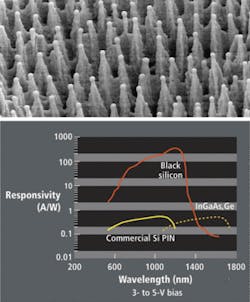
During this process, laser energy melts and re-solidifies the top surface of the silicon wafer, trapping quantities of sulfur from sulfur hexafluoride gas in the solid material, thus doping the semiconductor. In addition, the physical surface of the silicon is transformed from a smooth shiny wafer into a microstructured surface, yielding a material with a spectral response from 400 to 2500 nm and increased responsivity 100 times that of conventional silicon.
To commercialize this technology, SiOnyx (Beverly, MA, USA;www.sionyx.com) has licensed the Harvard black silicon patents in exchange for an equity position in the company. Because the sulfur implant used in the SiOnyx process is compatible with established semiconductor manufacturing processes, the black silicon process can be integrated with both frontside- and backside-illuminated imaging architectures.
Black silicon exhibits photoconductive gain at low voltage, producing multiple carriers from a single photon, similar to the effects produced in II-VI semiconductors or avalanche photodiodes under a high reverse-bias voltage where ballistic electrons generate additional charge. This phenomenon results in extremely high-quantum efficiencies of 10,000% and optical detectors with 100x improvement in photo-response at 3-V operational voltage. This 100x responsivity would enable a 1-μm square pixel to generate the same signal as a 10-μm square pixel under equal illumination conditions over the visible and near-infrared spectrum.
SiOnyx has already developed a fully integrated CMOS process flow and manufactured parts to validate the performance of the manufacturing process in two US-based CMOS foundries. Electrically, the 5-V operating voltage of the black silicon process enables direct integration with wafer-based CMOS processes and other analog and mixed-signal electronics without the need for any voltage isolation techniques to be used.
To integrate the technology into these processes, SiOnyx is currently working with a number of CMOS imager vendors to develop point, linescan, and area-array detectors based on this technology. Because the shallow junction process is tunable, SiOnyx can produce silicon detector and photovoltaic devices that respond from 400–2500 nm, covering the visible and solar spectrums and the short-wavelength infrared bands used in night vision, industrial, scientific, and medical imaging applications. In addition, because the technology increases the absorption of silicon, enabling the capture of visible and IR photons within 0.5 µm, crosstalk and infrared sensitivity issues are reduced.
IMAGE PROCESSING: Smart robots use sophisticated sensors
Basing their work on the basic functions of the insect brain, a European team of researchers have developed an architecture for artificial cognitive systems that could increase the ability of robots to react to changing environmental conditions and to learn behavior in response to external stimuli. The research team funded by the European Union’s SPARK project (www.spark.diees.unict.it) calls their architecture a spatial-temporal array computer-based structure (SPARC).
Within the SPARC software architecture, the robot’s powers of perception are enhanced by its ability to use information derived from visual, audio, and tactile sensors to form a dynamically evolving pattern. This pattern then determines movement of the robot. The cognitive system allows the device to autonomously “learn” based on a combination of basic reflexive behaviors and feedback from external environmental data.
“The robot initially behaves by primarily using basic inherited behaviors,” says Paolo Arena, the project coordinator. “Higher knowledge is then incrementally formed in the higher layer of the architecture, which is a neuron lattice based on Reaction Diffusion Cellular Neural Networks (RD-CNNs).” These RD-CNN processors are analog, parallel processors characterized by reactions in which two processes combine to create a third (http://en.wikipedia.org/wiki/Cellular_neural_network).
To extract salient features within images and allow them to be processed and fused with other sensor stimuli, researchers used the Eye-RIS 1.2 vision system from AnaFocus (Seville, Spain;www.anafocus.com). Shown for the first time at last month’s VISION trade fair in Stuttgart, the Eye-RIS vision system employs a hierarchical approach to image processing that splits image processing into image preprocessing and image post-processing. Image preprocessing extracts information from the input image, eliminating all redundant information using image convolutions, spatial filtering, and morphological and statistical operations. Image post-processing is used to perform more complex decisions and support action-taking using algorithms within long and involved computational flows.
The AnaFocus Eye-RIS vision system’s internal architecture accomplishes this using a Smart Image Sensor (SIS), a device similar to a CMOS image sensor but one where each pixel includes analog and binary processors and memory in addition to the optical sensor (see figure). Thus, each pixel in the SISs can both sense the corresponding spatial sample of the image and process it in close cooperation with other pixels.
Advances made in the SPARK project have also led to a number of software innovations in machine perception. The cognitive visual algorithms designed by the researchers have, for example, already been integrated into software from Hungary-based AnaLogic Computers (Budapest, Hungary;www.analogic-computers.com), a partner in the project. Recently, the company launched its InstantVision software package based on proprietary Cellular Visual Technology (CVT) that enables real time, bio-inspired, and massively parallel visual computing. The fundamental algorithms the company developed in SPARK, such as foreground and background separation, are integrated into the InstantVision package and can be used in applications including security surveillance.
The work of the SPARK project is continuing with the SPARK II project, which will more deeply research the details of insect brain neurobiology to refine, assess, and generalize the SPARC cognitive architecture. Following a background phase, performed in the SPARC, where relevant centers in insects and different types of spatial-temporal dynamics were investigated, SPARK II will introduce a computational infrastructure mimicking insect brain architecture. This will be assessed, optimized, and applied to different robotic structures to prove its generality. The architecture also aims to exploit a number of different sensors, including visual sensors to process perceptual processes as emerging image pattern and image understanding.
MACHINE-VISION SYSTEM: Smart camera performs glass bottle inspection
Glass is made when a mixture of silicon oxide, sodium carbonate, calcium oxide, magnesium oxide, and other minerals is heated to a temperature well over 1000°C. If the glass is intended for containers such as bottles, the molten glass is pressed into molds and then slowly cooled in a temperature-controlled kiln. At this point, inspection is performed on the glass.
Though contemporary production methods benefit from greater scientific knowledge of the properties of various additives to improve glass durability, the manufacturing process is far from perfect. Finished glass can contain bubbles or cracks, so each piece must be inspected by automated inspection systems.
When called on to retrofit an existing glass bottle inspection system for one of his customers, Thorsten Gonschior, president of Spectral Process (Erkelenz, Germany;www.spectral-process.de), developed a smart-camera-based system called the Opening Inspector to check the opening of hollow glass bottles for cracks, bubbles, and pressed artifacts.
“Keeping defective bottles off a production line is essential for the beverage industry. Anything but a smooth surface can cause injuries. Carbonated beverages might go flat or explode if the bottles have defects and can’t be sealed properly,” he says, “and each bottle must be free of burrs, chips, or sharp edges if it is to pass inspection.”
At the core of the system, the Opening Inspector uses an Iris P-Series camera from Matrox Imaging (Dorval, QC, Canada;www.matrox.com/imaging) to interface to sensors on the production line, perform visual inspection, and update actuators using the camera’s digital I/O interface. To measure the container’s inner and outer diameters and locate the cracks, bubbles, and over-pressed structures, the software uses metrology, edge detection, and blob analysis modules from the Matrox Imaging Library (MIL). Although the eye can easily distinguish over-pressed structures, high-contrast images are required for the software to detect them (see figure).
“Both the glass and its shape create illumination challenges,” says Gonschior. On a microscopic level, glass is nonuniform and any irregularities affect the way the light reflects and refracts through the surface. Resulting images can show strong contrast in the background microstructure. The roundish bottle shape and deviations in the bottle’s wall thickness only compound the problem.
Gonschior resolved many of these illumination issues by developing a custom light source that uses diffuse light to increase the contrast of any regions within the glass that contain cracks or bubbles. While the Opening Inspector system works with glass of any color, adjusting the intensity of the illumination device creates the right conditions to acquire a high-contrast image.
Using the camera’s Ethernet connection, a number of subsystems can be integrated into the inspection system, such as 2-D actuators to control labeling arms. Should manufacturers wish to inspect more than 400 containers per minute, the scalable design of the Opening Inspector allows additional cameras to be incorporated.
Once Spectral Process is satisfied with the Opening Inspector’s stability, the company plans to offer additional inspection stations. These will inspect the side walls and the bottom of glass bottles for defects and read barcodes and human-readable text.
ELECTRONICS MANUFACTURING: Open-source software targets SMT nozzles
In the production of printed circuit boards (PCBs), boards are first screen printed and solder paste or epoxy is applied. After entering a pick-and-place system, fiducials on each board are located to accurately determine where to place each of the surface-mount components. Pick heads mounted with vacuum-based pick nozzles then select individual components from component feeders and place them onto the PCB. When all the components are attached, the boards are transferred to a reflow oven for curing.
Because of the high speed and frequency with which these nozzles are used, they have a relatively short lifespan and must be periodically checked for general wear, defects, or other damage. To automatically detect defects and damage of the industrial nozzles used in the surface mount technology (SMT) industry, Fabio Caparrelli of the Materials and Engineering Research Institute (MERI) at Sheffield Hallam University (Sheffield, UK;www.shu.ac.uk) has developed a microscope-based machine-vision system using open-source software. This machine can be used to perform quality checks on individual nozzles to determine which nozzles have to be rejected.
MERI’s machine-vision system uses a FireWire camera attached to a Nikon SMZ800 optical microscope. Rather than use one of many commercial machine-vision or image-processing packages for image analysis, Caparrelli decided to use the HornetsEye toolkit available from the Microsystems and Machine Vision Laboratory at Sheffield Hallam. This open-source object-oriented software is a Ruby extension for real-time computer vision and allows the rapid prototyping of machine-vision applications through the Ruby scripting language.
“HornetsEye allows the fast development, implementation, and testing of the entire software program, in contrast to other more traditional packages written in C and C++ that require lengthy compilation,” says Caparrelli. Available atwww.wedesoft.demon.co.uk/hornetseye-api/, HornetsEye can be used to develop video and real-time computer vision under GNU/Linux (www.gnu.org) and provides interfaces to perform imaging and machine-vision applications. According to Caparrelli, the software can also be used in robotics, industrial automation, and microscopy and life science applications.
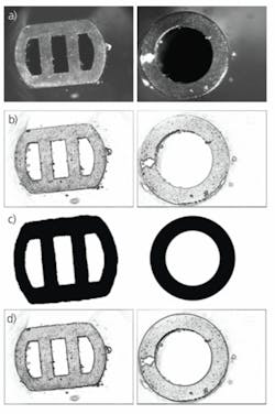
After images were captured into a host PC, several image-processing algorithms were used to identify defects and wear on the SMT nozzles. To determine whether any material chipping or erosion had occurred and detect the presence of dirt in the nozzles’ cavities, a number of different algorithms were used. To adjust for varying light conditions and noise in the acquired images, a Gaussian filtering algorithm was applied. As well as adjusting for different lighting conditions, the adaptive smoothing algorithm extracted the bottom face of the nozzle’s tip from the rest of the image (see figure).
To detect shape deformation as well as the presence of dirt, object templates of the nozzles’ tips were first created by digitizing known good images. “Alternatively,” says Caparrelli, “these templates could have been generated using CAD models of each of the parts, if they had been available. This would have eliminated the need to digitize the images of the known good parts.”
After these known good templates were generated, standard template matching techniques were used to detect the edges within the images, allowing any deformation in the nozzles to be seen. “Any possible object shape variations therefore provide a quantitative measure that can be used to classify the nozzle as good or bad. Alternatively, edge detection methods could have been used to compare the edges derived from both the templates and the real images.”


