Under the Hyperspectral Microscope
Hyperspectral imaging allows detailed examination of LED structures in the visible and near-IR
Over the last ten years, LED illumination has gained greater acceptance by machine-vision system developers looking for low-cost, long-lifetime lighting solutions; it has also grown into other markets such as home lighting. The major drawback of LEDs is that they are currently fabricated using expensive III-V materials. The manufacture of silicon-based LEDs will be a major breakthrough, as the material is cheaper to produce than III-V substrates. Realizing this, researchers at the University of Twente are using a hyperspectral microscope to study the effects of new LED designs on silicon.
In lateral LED structures, a gate electrode of polysilicon is placed above the active, light-emitting region (see Fig. 1). Operating the diode with constant current and a negative gate bias changes the intensity profile of the radiating surface allowing light emission to be varied.
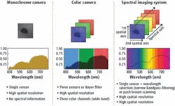
To understand this mechanism, the measurement of light-intensity data across the surface must be complemented by the spectral distribution of various frequencies of light across the diode structure. A hyperspectral microscope is required to performs these measurements. Using the microscope, measured x and y coordinates and the emitted radiation at certain frequencies can be mapped in a 3-D data-space cube (see Fig. 2).
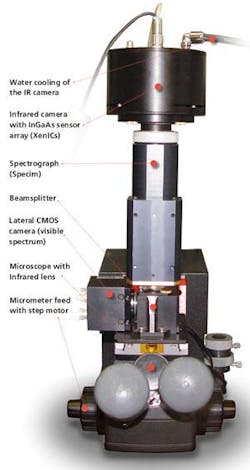
Jointly developed by XenICs and Twente University, the hyperspectral microscope is used to study light-emitting semiconductor structures in the IR region (see photo). In operation, a beamsplitter deflects about a third of the radiation to a laterally positioned CMOS camera, which is used to direct the microscope and select the surface portion of interest on the test object.
Multispectral data
The probe station allows easy selection and access to the device under test (DUT). In the station the camera port on top of the binocular microscope is used for mounting the hyperspectral system. This ensures that the electrical probe of the DUT is in line with the optical system. In this way the emitted overall light power and the spectral power density can be studied as a function of electrical power, gate-biasing, design geometry, and temperature.
Figure 2. Using a hyperspectral microscope, measured x and y coordinates and the emitted radiation at certain frequencies can be mapped in a 3-D data-pace cube.
To allow multispectral data to be captured by the system, the beamsplitter directs the remaining light through to an imaging spectrograph from Spectral Imaging Limited Specim. The company’s ImSpector is an optical add-on component designed to allow a 900- to 1700-nm linescan IR camera to operate as a spectral line imaging device. The IR lens of the microscope projects one line of the surface to be measured onto the spectrograph, which performs a spectral dispersion of the impending light and projects the spatial axis and the perpendicular spectral axis onto a near-IR area-scan camera sensor.
The software-configurable near-IR digital camera developed by XenICs and used in the microscope incorporates an InGaAs focal-plane array that can measure wavelengths from 900 to 1700 nm. Positioned on top of the spectrograph, the IR camera is cooled by a water-cooled Peltier element that works within the camera head. The camera head is then interfaced to a PC using USB 2.0 for control signals and Camera Link for 14-bit image data.
Camera setup
Two different measurement setups are used to direct surface capture and perform spectralanalysis using the microscope. The XenIC X-Control graphical user interface allows different camera functions such as integration time, operating temperature, uniformity correction and bad-pixel replacement to be set.
To adjust and select the scan of the LED to be examined, the laterally mounted CMOS camera is used. Here, too, X-Control is used to adjust the camera’s parameters, control the scan procedure, and generate a 3-D data set of x, y, and spectral coordinates in RAW format. Images are then evaluated using the environment for visualizing images from ITT Visual Information Solutions.
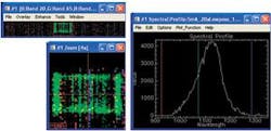
Figure 3. Output from a spectrograph is shown pseudocolored (left) and magnified (middle) along with its spectral profile (right).
One of the first images captured by the hyperspectral microscope shows a spectral analysis of the LED structure of Fig. 1 (see Fig. 3). Output from the spectrograph is shown pseudocolored and magnified along with its spectral profile.
Acknowledgment
The authors thank Jisk Holleman for his valuable contribution.
Bob Grietens is CEO of XenICs, Leuven, Belgium; www.xenics.com; Sander Smits is a researcher at University of Twente, Enschede, The Netherlands; www.utwente.nl.
null


