Machine Vision's Future Centers on CMOS and Consumer Advances
Andrew Wilson, Editor
More than a quarter of a century ago, the emergence of the CCD as a replacement for tube-based imagers, the IBM PC as a multipurpose computer, and general-purpose programming languages such as C, as well as the commercialization of technologies such as the LED, heralded the beginnings of the machine-vision industry as we know it today.
Perhaps the most important driving force behind the growth of machine vision and image processing has been the demand for low-cost systems that incorporate sensor, processing, and lighting components in high-volume consumer products.CMOS image sensors now inhabit every cell phone, LED lighting is commonplace in many automobiles, and embedded processors are now to be found in televisions, tablets, and toys. Leveraging these low-cost components has allowed machine-vision vendors to reduce the cost of their products.
Twenty-five years ago, a single machine-vision system designed to perform a simple inspection task may have cost $100,000. Today, a similar system based around a smart camera can perform the same task for $3000. While it may appear that the machine-vision industry has matured, the demand for products to address application-specific markets continues to drive the development of increasingly specialized OEM components.
More CMOS imagers
In the development of their latest generation of CMOS imagers, vendors now offer sensors with megapixel photosites, programmable regions of interest, multiple readout windows, and high dynamic range. To improve the low-light-level performance of these devices, many companies are already employingbackside illumination (BSI) techniques.
Indeed, Yole Développement (www.yole.fr) predicts that although BSI sensors will only account for 18% of total CMOS image sensors this year, a fast adoption of the BSI technology is expected to reach more than 50% by 2017. Over this same period, the CMOS image sensor market is expected to grow at an 11% compound annual growth rate from $6.6 billion in 2012 to $11 billion in 2017.
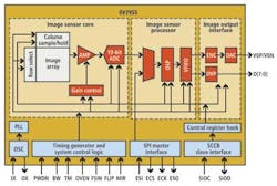
Although much of this growth will be spurred by the use of low-cost CMOS imagers in smart phones and tablet computers, smart cameras designed for automotive and security applications will drive the demand for integrated image capture and processing devices.OmniVision has already developed an integrated image sensor, the OV7955, that combines an image sensor, on-chip digital signal processor (DSP), and image memory designed for rear-view mirror automotive applications (see Fig. 1).
Taking a more modular approach, the latest Xarina CXD4135GG and CXD4235 systems-on-chip (SoCs) fromSony integrate image signal-processing functions and video encoding for the next generation of IP surveillance cameras that use the company's ICX692AKA color CCD and IMX140LQJ CMOS image sensors. Large-volume OEMs will leverage the power of combined image sensing and processing products either by purchasing standard products such as OmniVision's or by commissioning CMOS imaging developers to build custom devices.
For lower-volume applications, such as specialized machine-vision tasks, using CMOS imagers with attached co-processors will remain the most cost-effective architecture of choice. Having said that, the nature of these co-processors themselves is changing, with field-programmable gate array (FPGA) and digital-signal processor (DSP) vendors alike offering increased levels of sophistication (see "Low-cost embedded devices boost end-user applications," this issue). Likely as not, vendors will use these products in their next-generation smart camera systems, increasing the processing capability of their products.
Product differentiation
To further differentiate their products, camera vendors will need to leverage the advances being made in CMOS device technology and optical components. This will allow them to address more specialized vision applications in semiconductor inspection and life sciences. Working with a major national laboratory, Alacron, for example, has developed a number of deep-ultraviolet cameras based on backside-illuminated CMOS imagers (see "DUV cameras target semiconductor inspection applications," Vision Systems Design, September 2012).
To address the needs of scientific and automotive applications, a number of different CMOS architectures have been proposed, including dual slope, logarithmic, and techniques such as those used in scientific CMOS (sCMOS) devices and cameras from companies includingAndor, Hamamatsu, and PCO that use dual gain amplifiers to increase the dynamic range of these devices.
Filter patterns
Applying different color filter patterns is another way CMOS vendors will differentiate their products. Rather than use the traditional Bayer pattern, the Truesense color filter fromTruesense Imaging adds panchromatic pixels to the standard RGB pixels traditionally used for color capture to increase the intensity of captured images. It may only be a matter of time before the company offers this technology on its latest 12-kpixel, 100-frames/sec QFHD CMOS image sensor.
Other methods to increase the amount of light captured by CMOS imagers are also under development. At InVisage, engineers have developed a method to apply a coating of quantum-dot material on a CMOS silicon wafer. The company's web site claims this so-called QuantumFilm has allowed it to build "the world's most sensitive mobile camera with four times the performance of today's CMOS imagers."
Others, most notably the Fraunhofer Institute for Integrated Circuits, have shown how polarizing filters can be used with conventional CMOS imagers to develop cameras for materials stress testing (see "Smart camera measures stress in plastics and glass," Vision Systems Design, January 2012). Extrapolating this idea, it is likely that in future filter patterns may incorporate infrared (IR) or even UV filters to produce single-chip multispectral imagers.
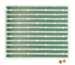
Adding to this diversity, ISORG is one of the pioneers of a new breed of large-area organic image sensors that will be developed using a matrix integration of rows and columns of photodiodes. According to ISORG, these image sensors will transform plastic surfaces into smart surfaces that can recognize object position, movement, and shape all over the surface or be used to convert glass surfaces into smart surfaces that scan and copy documents (see Fig. 2).
Miniature components
Much research is also currently underway in the development of miniaturized lenses for CMOS imagers. Just last year, IMEC demonstrated a novel way of producinghyperspectral imagers by replacing the traditional optics of current systems with on-chip optics and a tunable microelectromechanical system (MEMS).
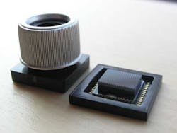
At the Fraunhofer Institute for Applied Optics and Precision Engineering (IOF), Frank Wippermann and Andreas Brückner have shown howmicrolens fabrication techniques can dramatically reduce the size of lenses for VGA imagers. Instead of using a single-aperture lens, the design transfers fractions of the full field of view (FOV) through different optical channels, thus requiring only a single lens with a short focal length for each (see Fig. 3).
Other, perhaps more futuristic ideas include a recent proposal by Sony that has patented a method of using back-illuminated CMOS image sensors thinned to micron thicknesses, which, if bent into the shape of an eye, could capture wide-angle images.
While the integration of sophisticated sensors and processors will reduce the cost of camera systems, the adoption of active cables for camera-to-computer interfaces is allowing connections at increasingly longer distances (see "Clearing Up Choices for Cabling and Connectors," Vision Systems Design, September 2012).
Leveraging standards
To extend these distances further, more expensive optical repeaters can be used. However, the adoption of standards such as IEEE 802.11n and the future 802.11ac standard will allow 1-Gbit/sec images to be transferred wirelessly between camera and computer systems.
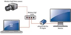
At last month's VISION 2012 tradeshow in Stuttgart,Pleora Technologies demonstrated its GigE Vision over wireless IP engine being used to transfer images losslessly from an IR camera to a host PC (see Fig. 4). According to president George Chamberlain, the company is currently working on customer-specific implementations for the technology and will offer general-purpose interfaces as OEM boards and IP in 2013 next year.
While such systems will not challenge the data rates offered by Camera Link, CoaXPress, and USB 3.0 standards, they will reduce the baling required in applications such as intelligent transportation systems where cameras are often mounted on gantries. In these systems, the adoption of consumer lens standards such as theMicro Four Thirds standard (MFT) will allow camera vendors to provide remote auto-zoom, auto-focus, and auto-iris adjustment (www.four-thirds.org/en/microft/).
Originally developed by Olympus and Panasonic to reduce the size and thickness of mirrorless interchangeable lens digital cameras and camcorders in the consumer market, the MFT standard has already been used bySVS-Vistek in a prototype GigE Vision camera first demonstrated at the 2012 VISION show. By incorporating the MFT interface, zoom, iris, and focus can be controlled remotely over the GigE Vision interface.
Drawing from consumer goods
Wireless standards and consumer lens standards will increase the range of camera manufacturer offerings; the use of consumer products themselves will also impact future vision system designs. Based on range camera technology developed by PrimeSense, Microsoft's Kinect is already finding multiple uses in applications that vary from robotic guidance to medical imaging (see "Kinect API Makes Low-Cost 3-D Imaging Systems Attainable," Vision Systems Design, October 2012).
Needless to say, with the success of the Kinect, other products, most notably the Leap from Leap Motion (https://leapmotion.com) and WAVI Xtion from Asus (http://event.asus.com), are vying for a share of the imaging market. In future, perhaps a similar product will emerge from Apple Computer (www.apple.com) that already has a patent filed on the concept (http://1.usa.gov/s0UQC9).
Companies Mentioned in this Article
Alacron
www.alacron.com
Andor
www.andor.com
Fraunhofer Institute for Applied Optics and Precision Engineering
www.iof.fraunhofer.de
Fraunhofer Institute for Integrated Circuits
www.iis.fraunhofer.de
Hamamatsu
www.hamamatsucameras.com
IMEC
www.imec.be
InVisage
www.invisage.com
ISORG
www.isorg.fr
Olympus
www.olympusamerica.com
OmniVision
www.ovt.com
Panasonic
http://panasonic.com/
PCO
www.pco.de
Pleora Technologies
www.pleora.com
PrimeSense
www.primesense.com
Sony Component Solutions Business Division
www.sonycsbd.com
SVS-Vistek
www.svs-vistek.com
Truesense Imaging
www.truesenseimaging.com
For comprehensive listings of component vendors by category, visit theVision Systems Design Buyer's Guide.

