OPTICS: Microlenses make miniaturized closeup imaging a reality
By mounting specialized optics onto commercially available CCD and CMOS imagers, researchers are developing low-costminiaturized imaging systems to tackle applications ranging from multispectral analysis to stress testing and biomedical imaging. The cost of optically smart cameras will be drastically reduced as a result of eliminating a number of optical components used in the traditional imagers previously used to perform these tasks.
Last year, IMEC (Leuven, Belgium;www.imec.be) demonstrated a novel way of producing hyperspectral imagers by replacing the traditional optics of current systems with on-chip optics and a tunable microelectromechanical system (MEMS). By effectively replacing the slit and collimator of traditional multispectral cameras, the novel devices can operate at approximately 10k lines/s (see "Novel technology lowers the cost of hyperspectral imaging," Vision Systems Design, January 2011).
To achieve a similar cost reduction in cameras designed for materials stress testing, Fraunhofer Institute for Integrated Circuits (Erlangen, Germany;www.iis.fraunhofer.de) has developed the Polka camera. A conventional CMOS image sensor of 1120 × 512 pixels is overlaid with a 2 × 2 matrix of polarizing filters. In this way, relative stress levels within an object at speeds as fast as 250 frames/s can be measured (see "Smart camera measures stress in plastics and glass," Vision Systems Design, January 2012).
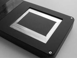
Now, Andreas Brückner and his colleagues at the Fraunhofer Institute for Applied Optics and Precision Engineering (Jena, Germany;www.iof.fraunhofer.de) have demonstrated a micro-optical imaging system for high-resolution applications in biomedical and industrial applications (see Fig. 1).
Integrating a microlens array with an off-the-shelf image sensor, the system achieves a resolution of approximately 3000 dpi across a 36.1 × 24-mm array with object-to-image distances as short as 5.3 mm. By decoupling the tradeoff between system length and field-of-view size, the compact imaging system captures a two-dimensional object field at the size of the image sensor array itself.
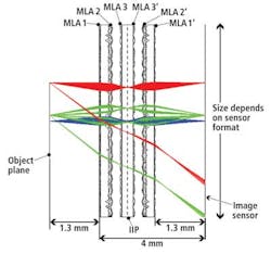
The system consists of six microlens arrays axially aligned in a symmetric fashion. In each optical channel, the first and second microlens arrays (MLA 1 and MLA 2) produce a demagnified, inverted image of the respective part of the object in the intermediate image plane (IIP). A reversed group of the same microlenses relays the intermediate image onto the final image plane (see Fig. 2).
Since each partial image has unity magnification, a total image of all partial images results in a complete reconstruction of the final image. The size and possible overlap of adjacent partial images is controlled by the field diaphragm array, which lies in the center of axial symmetry. Additional field lens arrays (MLA 3 and 3') control vignetting and suppress crosstalk.
This micro-optics and image sensor assembly is integrated in a modified GE4900, 4872 × 3248-pixel CCD camera fromAllied Vision Technologies (Ahrensburg, Germany; www.alliedvisiontec.com). Brückner and his colleagues tested the system by capturing an image of a chrome-on-glass USAF 1951 test pattern using an LED backlight realized by an external light source. This resulted in a measurement of approximately 3000 dpi across the extended object field.
In the future, Brückner plans to integrate frontside illumination to enable the ultracompact closeup imaging system to be used in applications such as industrial inspection, quality assessment, and biomedical imaging.


