Andrew Wilson, Editor
Today's portable cell phones, tablets, and electronic devices require increasingly smaller printed circuit board (PCB) footprints. At the same time, installed semiconductor processing equipment such as screen printers, chip placement systems, optical inspection units, and reflow ovens have been designed to handle much larger PCBs such as PC motherboards.
To take advantage of this legacy semiconductor equipment while at the same time increasing the throughput of smaller PCBs, manufacturers have turned to a process known as panelization. Here, a number of identical circuit boards are printed onto a large panel that can be handled by existing equipment. After processing, these panels are then separated for final testing.
"Unlike single motherboards that may require reading a single barcode," says Steven King, Senior Solutions Engineer for Electronics at Microscan (Nashua, NH; USA; www.microscan.com), "each individual panel and each of the multiple circuit boards that it contains must each have a unique barcode identifier." In this way, each individual circuit board can be identified with each panel as the PCB panel moves through the production process.
In this process, barcode labels (or codes laser marked onto the individual boards within a panel) are affixed to the panel and individual circuit boards before the screen printing process. To ensure that each of these panels and the individual circuit boards they contain can be tracked though the entire process, these barcodes must be read after they are affixed or marked.
Differing approaches
"In the past," says King, "this was often accomplished by an operator using a handheld barcode scanner -a process that was time consuming and subject to human error. To automate this process, PCB manufacturers can incorporate automatic barcode readers that can read the panel and circuit codes after they are affixed or marked.
"One approach to performing this task automatically," says King, "is to use an array of cameras or barcode readers that are positioned over specific areas of the board where the barcode will be known to be affixed. While this solution is effective when large batches of the same product are being manufactured it is not flexible since, should a new batch of panels with different-sized circuits need to be processed, the positions of each of the cameras or barcode readers must be reset.
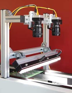
To overcome this limitation, while at the same time increasing throughput and eliminating human error, Microscan has developed a line-scan-based machine vision system known as PanelScan (Figure 1). Capable of being mounted to most in-feed or transport conveyors, PanelScan will be offered in two versions. The first, PanelScan Standard, incorporates a single line-scan camera and is capable of scanning PCBs as wide as 10 in while the second, PanelScan Wide, features a dual line-scan camera combination capable of scanning boards of 18 in width.
Line-scan cameras
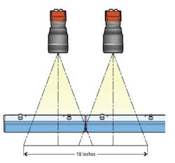
In the design of the PanelScan Wide system, two raL6144-16gm Racer line-scan Gigabit Ethernet cameras from Basler (Ahrensburg, Germany; www.baslerweb.com) are mounted on a gantry 13 in from the PCB. Both cameras are fitted with an AF 60mm Nikor lens from Nikon (Melville, NY; USA: www.nikonusa.com) that allow each camera to scan a 10 in swatch across the PCB as it moves though the system. To ensure that the entire 18-in swath is scanned, each camera is positioned so that the field of view of each camera overlaps by 1in (Figure 2). "This configuration," says King, "allows the system to read standard barcodes as small as 3.3 mil or Data Matrix 2D codes as small as 5 mil."
To illuminate the PCB as it moves under the cameras' field of view, Microscan has incorporated two of the company's own NERLITE HI-BRITE LL-300 Series white line-lights into the system. Mounted in an off-axis configuration, these 300 mm lights are butted together to form a seamlessly white line-light that illuminates the PCB as it moves under the field of view of the dual-camera system.
As a board moves through the system, its leading edge is detected by a retro-reflective sensor from Tri-Tronics (Tampa, FL; USA: www.ttco.com), the output of which is used to trigger the scanning process. Images are then transferred over each cameras Gigabit Ethernet interface to a host PC. This data is buffered to the PC in 256 line segments of each 6k x 1 scan. Transferring fifty of these 256, 6k x 1 line segments from both cameras results in an image of 12k x 12k x 8-bit pixels.
Image analysis
This data must then be processed to detect both the barcode on each panel and the individual barcodes associated with each individual circuit board. To perform this task, Microscan has incorporated its Visionscape machine vision software package into the system. In addition to incorporating automatic identification tools for decoding linear and 2D codes, the software also incorporates an array of image enhancement and analysis tools. However, just as important as the software tools that are used to perform barcode detection is the graphical user interface that Microscan has developed for the PanelScan system.
"In the development of the GUI," says John Agapakis, Director of Americas Sales at Microscan, "it was necessary to provide an easy method of both configuring the system and providing fast barcode reading without the operator requiring any knowledge of machine vision software."
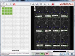
Specifically, each batch of PCBs panels may contain a number of different circuits in an array of multiple rows and columns (Figure 3). While some panels may contain twelve circuits configured in a 3 x 4 matrix, others may contain many more. To identify which type of panel is desired to be inspected, the GUI allows the operator to enter this matrix format before the panel is scanned. After this data is entered, a single panel is scanned through the system in teach mode. After scanning the complete image of the panel, each of the circuit boards is automatically processed to increase the contrast and the image displayed on the GUI.
After this operation is complete, the operator highlights the center portion of the top left and bottom right barcode within the image. The system then automatically searches in all the regions for the barcodes located on each of the individual circuits and reads each individual barcode. Data from all of the barcodes is then concatenated into a string and stored in the host PC. After this process is complete, multiple PCB panels of the same configuration can be run through the system at a rate of approximately one board per second.
Throughout the teach process or the subsequent run-time operation of the system, no specific machine vision knowledge is required from the operator.
Track and trace
"Of course," says King, "while barcode reading is important to perform in the initial stage of PCB fabrication, it is equally important to monitor the panels and circuits as they move through solder paste inspection, IC placement, automatic optical inspection, and solder reflow. However, at these stages, it is no longer necessary to read each of the barcodes associated with each panel and circuit since these identifiers are all related. "
Thus, it is only necessary to perform a single barcode read at each of these stages to determine which panels and circuits are being processed. This task can be performed with a single smart camera or barcode reader at each of these stations. To date, the PanelScan system has been recently validated at a number of PCB manufacturers including a Tier I automotive electronics manufacturer and a Top Ten Global EMS (Electronics Manufacturing Services) company, according to Agapakis. While the system is currently configured to read barcodes on PCB panels and circuits, it could be equally well deployed in systems in semiconductor applications where trays of ICs need to be inspected.
Companies Mentioned
Basler
Ahrensburg, Germany
www.baslerweb.com
Microscan
Nashua, NH; USA
www.microscan.com
Nikon
Melville, NY; USA
www.nikonusa.com
Tri-Tronics
Tampa, FL; USA
www.ttco.com
Vision Systems Articles Archives
About the Author

Andy Wilson
Founding Editor
Founding editor of Vision Systems Design. Industry authority and author of thousands of technical articles on image processing, machine vision, and computer science.
B.Sc., Warwick University
Tel: 603-891-9115
Fax: 603-891-9297


