Automated vision system checks surface mount components
An automated vision system enables surface mount capacitors to be inspected at a rate of six per second.
Mike Phillips
Over the past several decades, surface mount technology has become the preferred means by which small components are mounted onto printed circuit boards. As the technology has increased in popularity, it has replaced older through-hole technology that involved inserting components with leads into holes drilled in a circuit board and soldered to pads on the opposite side.
Today, surface-mounted components (SMCs) such as resistors and capacitors are used in large quantities in the manufacture of all forms of electronic equipment. Although they perform the same function as their leaded predecessors, their construction is markedly different - instead of leads, they feature metal connections at either end. As such, they are smaller than their leaded counterparts and easier to place using automated assembly equipment.
Traditionally, inspecting the quality of SMCs was an offline process performed by removing a number of components from a batch and manually inspecting them under microscopes. However, this is labor intensive and prone to operator fatigue. What is more, the quality of every component in a given batch cannot be assured.
Automated process
To fully automate the quality inspection process for one leading capacitor manufacturer, engineers at Envisage Systems (Bletchley, Buckinghamshire, UK;www.envisagesystems.co.uk) were called upon to develop a vision-based system that would inspect the basic dimensions and integrity of all the company's chip capacitors at a rate of approximately six per second.
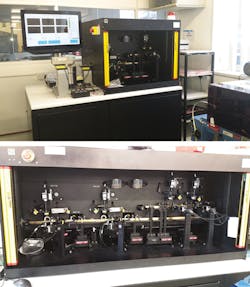
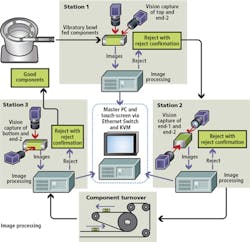
The CAPVIS system (Figure 1) comprises a set of three independent PC-based vision stations, each with a pair of cameras that communicate with a master PC fitted with a touch screen interface. While the three vision stations inspect the features of the SMCs, the main interaction with the system is through the touch screen interface on the master PC.
Between them, the three vision stations capture images of all six sides of a component, after which the system software calculates the overall component dimensions, the dimensions and total area of the termination pads, pad alignment and surface defects on both the capacitor body and the termination pads. To process the images, Envisage Systems chose to deploy the HALCON image processing library from MVTec Software (Munich, Germany;www.mvtec.com), which consists of a number of image processing operators that were incorporated into the C#-based applications running on each of the three vision stations.
In operation, SMCs of a specific type are first loaded into a vibratory bowl feeder. From the bowl feeder, they are carried down a linear accumulation track and onto the first of two toothed timing belts treated with an antistatic coating which prevents static discharge from destroying the components and precludes the parts adhering to one another. As the capacitors are separated by a distance of approximately 10mm, the belt carries each capacitor into the first of the three inspection stations.
Compounding the inspection process was the need to inspect specific types of SMCs with body faces of more than one color. Ideally, it would be preferable to initially orient the capacitors so that the same colored face would always be presented to the vision systems. However, to do so would reduce the inspection rate of the machine, since incorrectly-oriented components would first need to be identified and fed back into the bowl feeder prior to inspection. The alternative solution adopted was to identify the capacitors prior to performing any of the inspection checks.
Checking chips
As a capacitor enters the first of the inspection stations, an E3C-LD21 2M 7 and E3C-LDA51 2M photoelectric laser line sensor from Omron (Kyoto, Japan;www.omron.com) detects the presence of the capacitor on the belt and triggers a SpecBright RF1-000-I-H-F-1-00 LED ring light from ProPhotonix (Salem, NH, USA; www.prophotonix.com) and the first of a pair of acA1300-60gm 1.3MPixel cameras from Basler (Ahrensburg, Germany; www.baslerweb.com) fitted with an MML series telecentric lens from Moritex North America (San Jose, CA; USA; www.moritex.com) that capture a magnified image of the top surface of the capacitor.
A second horizontally-mounted Basler acA1300-60gm 1.3MPixel camera, also fitted with a Moritex MML series telecentric lens captures an image of one of the sides of the capacitors which is illuminated with a ProPhotonix RF1-000-I-H-F-1 in-line LED ring light. Both images are then transferred over a GigE interface to the first vision PC for processing (Figure 2).
Prior to any image analysis, the location of the chip in the image is first identified after which the body and the termination pads are identified. Next, the color of the top surface of the image of the capacitor is determined by the HALCON software to determine the appropriate set of image processing tools that should be used to further determine the characteristics of the part.
Having done so, the image of the top surface of the chip is processed to ascertain the length and the width of the chip body, the length and width of the termination pad and the gap between the termination pads. The image of the side view of the component, on the other hand, is processed to calculate the thickness of chip, the gap between the termination pads and the length between the termination pads.
The chip is also checked to ensure that there are no defects in the body. To do so, the image processing software looks for variations in hue variations and brightness. Hue defects occur where the color of the chip changes - for example where a green substrate shows through the body of the chip, while brightness defects arise where there are bright or dark areas on the body of the chip caused by excess termination.
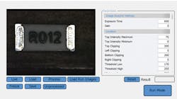
On some chip types, printed characters are present. Hence, it is important that the system identifies the characters so that they are not detected as defect areas when the system performs its body checks. Secondly, the approximate area covered by the characters must be checked to confirm that all of the characters are present (Figure 3).
If the SMC passes all the inspection processes, it is carried down the conveyor to the second of the inspection stations. If the chip fails, it is rejected from the belt. To do so, the PC instructs a pneumatic actuator to eject the part from the belt into a bin through a photoelectric reject confirmation sensor that verifies that the device has been removed from the belt.
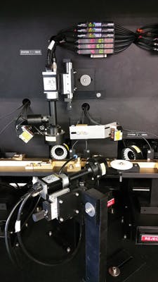
At the second of the three inspection stations, images of the sides of the surface mount capacitors are captured by a second pair of Basler acA1300-60gm 1.3MPixel cameras also fitted with MML series Moritex telecentric lenses that are mounted either side of the moving belt.
To orient the component so that its ends are facing the two cameras, a wheel was fitted to the belt which is driven in synchrony with it. As the capacitor contacts the wheel, it is rotated such that the ends of the capacitors face the two cameras in the system. Images from the two cameras are then transferred to the second of the three PCs in the system over a GigE interface where they are processed (Figure 4).
The end inspection of the termination of the capacitors is a somewhat more simplified procedure. Here, the HALCON vision software checks to determine that the ends have been coated with a uniform termination and no holes or gaps are present. If the device passes the second of the inspections, it is conveyed down the belt to the third and final inspection station. If not, the PC instructs a second pneumatic actuator to eject the device through a reject confirmation sensor into a reject hopper.
To inspect all six sides of a capacitor for defects, a novel mechanical means was developed to rotate the component by 180o so that the bottom and final side of the component could be inspected by the third vision system. To rotate the component after it leaves the second of the inspection stations, it is carried along the toothed belt until it comes into contact with a second belt which impinges upon the first. The component is then held between the two belts until it has been fully rotated. The component is then released between the two belts and continues along the second belt into the final inspection station.
The third and final inspection station replicates all the functions performed at the first station to inspect the bottom and second side of the capacitor. Once more, the length and the width of the chip body, the length and width of the termination pad and the gap between the termination pads are determined from the bottom of the device, while the thickness of chip, the gap between the termination pads and the length between the termination pads is calculated from the image of the side.
If the chip fails the final inspection it is removed from the conveyor into a reject bin through a reject confirmation sensor by a third pneumatic actuator. If the chip passes, it is conveyed further down the belt where it is ejected into a bin with the rest of the components that have passed all the inspections.
User interface
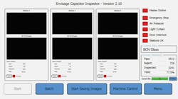
Three PCs are used to perform the image processing analysis functions in the system and all the user interaction with the system is performed though a custom-built touch screen interface which resides on the master PC. From the master PC, a user can select specific batch types, add new parts to be inspected by the vision system and save images from the inspection process. The master PC is also responsible for overall system control and ensuring that all safety circuits are enabled before any system operation is allowed.
During operation, images of the inspected parts from the vision stations, and the results of the analysis, are transferred to the master PLC over the Ethernet interface from where an operator can visually review the processes in the system (Figure 5).
If a part has failed the inspection process at any of the four stations, the master PLC highlights the location on the image where the failure is located.
The user interface also presents the overall statistics from the inspection process, including the number of parts inspected, how many have passed or failed and the overall yield. Similar statistics are displayed for each of the three stations.
From the data, an analysis can be performed to determine the nature of the most common failures, and whether any enhancements might be appropriate in the manufacturing process.
Should the manufacturer need to inspect a new batch of capacitors, the system can be trained to identify the key characteristics of the new devices- such as their width, length and location of the termination pads - through the hierarchical user interface.
Mike Phillips, CEO, Envisage Systems, Bletchley, Buckinghamhire, UK (www.envisagesystems.co.uk).
Companies mentioned:
Basler
Ahrensburg, Germany
www.baslerweb.com
Envisage Systems
Bletchley, Buckinghamshire, UK
www.envisagesystems.co.uk
Moritex North America
San Jose, CA; USA
www.moritex.com
MVTec Software
Munich, Germany
www.mvtec.com
Omron
Kyoto, Japan
www.omron.com
ProPhotonix
Salem, NH, USA
www.prophotonix.com
