Vision system tracks wafer processes
By Lawrence J. Curran
Contributing Editor
A 300-mm (12-in.) diameter semiconductor wafer represents a substantial investment for a device manufacturer because the wafer passes through numerous fabrication steps. Accordingly, device manufacturers carefully inspect the wafers through every processing operation. They need to know as soon as possible if a partially processed wafer has been damaged or whether process parameters have changed, drifted, or malfunctioned. If so, manufacturers must take immediate steps to correct problems, preventing further reductions in subsequent wafer yields.
To meet these inspection needs, vision systems are in widespread use in automatic wafer-identification applications reading alphanumeric-character strings and barcodes. In front-end fabrication, manufacturers track wafers to help pinpoint difficult process problems. Wafer identification is also used in back-end test and assembly steps, such as handling and probing, where it can verify that process steps and parameters match those of individual wafer requirements.
null
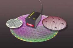
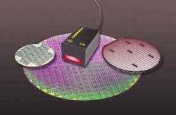
For example, Axcelis Technologies (Beverly, MA) has integrated an advanced wafer-identification reader—the In-Sight 1700 wafer-identification reader from Cognex Corp. (Natick, MA)—-into many of its latest ion-implantation systems used in semiconductor fabrication (see photo). Most of the Axcelis implanters being installed in 300-mm foundries worldwide are also equipped with the wafer reader, which is offered as an option by Axcelis.
Ion implantation inserts dopants into a wafer to tailor the performance of the individual device formed. In addition, a unique alphanumeric identifier is scribed onto each wafer so that it can be traced throughout processing. The challenge for the wafer reader is to reliably read the identifier at each fabrication step.
Subsystem integration
Cognex has already done some of the systems-integration work for OEMs who adopt the In-Sight 1700 by incorporating a CCD sensor, lighting, processor, and both serial and Ethernet communications capabilities into one housing. Gilbert Chiang, Cognex product marketing manager who worked on the In-Sight 1700 design, says most of the details about the elements comprising the unit are proprietary. However, the 640 × 480-pixel CCD array uses an image board and lens that are integrated by the company to form the sensor.
Lighting is provided by a board containing 160 red LEDs to deliver 11 different lighting modes; the board uses band selection that activates specific rows of LEDs to illuminate selected areas of a wafer. An on-board digital-signal processor accepts and executes commands from the other processors in the Axcelis ion-implantation system.
Chiang says Cognex supplies "standard Ethernet protocols with the reader, and we allow users to access a graphical user interface (GUI) via a Java applet. The applet serves up the GUI, which allows users to see what the scribe reader views." He points out that the scribe marks are made as small as 1 mm high and 3 mm wide so that the scribes occupy a very small wafer space, allowing more space for active devices.
Chiang adds that the wafer reader's algorithms are tailored to the Semiconductor Equipment and Materials International (SEMI; Mountain View, CA) standard 2-D, OCR, and barcode identification. The software allows users to read the T7 2D code and the SEMI M12 alphanumeric mark in the same field of view. The T7 2D is a standard for 300-mm wafers that covers the placement of scribes on the front and back sides of wafers within 5° of the wafer notch. (The notch on 300-mm wafers serves the same orientation function as the flat on smaller-diameter wafers, but does not subtract as much valuable space as a flat.)
Michael Laine, software product marketing manager at Axcelis, says his company needed to equip the implantation units with an intelligent wafer reader small enough to be accommodated in an extremely tight space among many complex moving parts. In addition, the reader had to be integrated into the implanter's distributed Ethernet-based control-system architecture. Moreover, the wafer reader also had to provide reliable data at every process step, regardless of variations in scribe appearance caused by chemical material polishing, copper metallization, or other process effects.
He describes the wafer reader's optics as "exceptionally good, allowing us to easily read markings on the back side of a wafer that's processed front and back." Laine adds that today's 300-mm foundries are highly automated, demanding fast throughput, "and our tool has to interact with a sophisticated [process control] system, sending data to a high-level computer."
Network compatibility
The In-Sight 1700's networking capability was also persuasive. "We were able to displace the incumbent wafer reader because the 1700 TCP/IP-based networking technology is compatible with the architecture of our implanters," Laine says. "Having that [capability] complements the higher-level architecture we use in our systems, enabling us to do better diagnostics when we want to do fault detection."
Axcelis had little difficulty integrating the wafer reader into its implanters. Laine says the compact design of the wafer reader allowed Axcelis to design a fixture that places the wafer reader strategically "in a place where we do a lot of work—near a dual-arm robot and a prealigner that orients the wafers using their reference notches before they enter the processing chamber."
The reader is mounted in the in-air portion of the wafer-handling subsystem, in close proximity to the process chamber that holds the wafers during implantation. As a wafer is transported into the reader's field of view, the reader first triggers the LED array to illuminate the edge of the wafer where the scribe is located. This lighting provides even illumination across the wafer surface without glare or "hot-spot" reflections.
Once an optimal image is formed, the scribe is read using character-recognition algorithms, and the identification (ID) data are transferred to the ion implanter's host-control program. "This is all done before the wafer is processed to make sure that if, for example, the ID reads "lot 500 and wafer 12," we know that wafer should be processed with the specific recipe assigned to that lot," says Laine.
Nor did software integration present any major hurdles, according to Laine. "Our software engineering team interfaced the reader into our distributed computing environment, learning the Cognex 'teach mode' quickly because of its built-in Web browser.
"All we had to do was connect a remote PC onto our Tools TCP/IP network router. Through this interface and the Cognex 'job' object, we were able to save time because of the large number of variables that can be assigned to a single job," Laine adds. For example, Axcelis combines both OCR and T7-type markings in a single job object, providing the flexibility to build a broad set of jobs that can cover variations in customer process recipes. Furthermore, during "full automation mode," the Axcelis automation subsystem computer can readily and intelligently communicate with the wafer fab manufacturing execution system, which, in turn, communicates all the appropriate information to the wafer reader to perform reads.
"We were able to integrate the reader into our [implanter's] control system, which is complicated because it has to control the timing of functions such as plasmas, vacuum, and wafer handling," Laine says. Any one of those steps can dictate that a signal be sent to the reader to perform a read scan and then send that digitized data back to the control system. Laine says, "Given all of those operations that had to work together, we had a relatively simple task to integrate the reader into our control system."
That control system comprises a Sun Microsystems (Santa Clara, CA) Ultra workstation running the Solaris operating system, a Windows NT-based PC, to which the wafer reader interfaces, and a cell controller. The operating system manages all of Axcelis' SEMI 300-mm automation software. The cell controller is an Axcelis-built single-board computer that runs the Axcelis system's VxWorks real-time operating system provided by Wind River Systems (Alameda, CA). All of these processors are bundled into the ion-implantation system.

