White-light interferometry enables MEMs inspection
Microelectromechanical systems (MEMs) can detect sudden shifts in pressure and movement and perform as micron-sized light switches. According to John Gordon, senior analyst at Venture Development Corp. (VDC; Natick, MA, USA; www.vdc-corp.com), revenues from MEMs and microstructure devices will reach $34 billion by 2006 on sales of 10.4 billion units, up from $17 billion in 2002 from 3.4 billion units. To test these devices, machine-vision systems must be capable of taking measurements of millionths of inches.
MEMs are manufactured in cleanroom environments using many of the same processes as those used for integrated circuits. MEMs features are typically 10 to 1000 times larger than the smallest features on a microchip; however, MEMs devices have large aspect ratios where the height of a structure may be many times its width, posing depth-of-field imaging problems. For example, a single ink-jet nozzle on a printer can be millimeters deep, but only a few tens of microns across. When in-line MEMs inspection is required, white-light interferometric imaging systems from companies such as Nano-Or Technologies Ltd. (Lod, Israel; www.nano-or.com) and NanoVia (Londonderry, NH, USA; www.nanovia.com) must be used to make wide-area, high-resolution 3-D measurements.
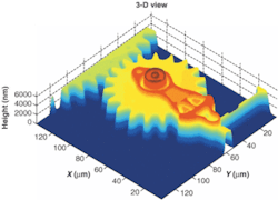
Proprietary optics coupled to a white-light microscope are used by Nano-Or to create a stable vibration-insensitive interferometric map of a 3-D surface of a MEMs wafer. In the system design, a proprietary optics scheme is coupled to an XGA-compatible Sony (Park Ridge, NJ, USA; www.sony.com/videocameras) monochromatic CCD camera and a PCVision Plus frame grabber from Coreco Imaging (Montreal, Quebec, Canada; www.coreco.com). Captured images are computed as 3-D surface quantitative maps with nanometer resolution. By using proprietary algorithms with off-the-shelf components, the Nano-Or 3-Dscope2000 can capture a full field of view in less than 1 s and can generate a 3-D map in 3 s, according to CEO David Banitt.
The Nano-Or 3-Dscope2000 system is insensitive to vibrations in the z-axis during measurement or probing of samples such as MEMs devices. Unlike most interferometric systems that require a reference beam in addition to the probe beam, the system uses a single light source. "MEMs are often host to wires for actuation. Movement during actuation does not disturb the inspection system, so that measurements of the devices under different settings is simple and accurate," Banitt says.
Similar approach
NanoVia takes a similar approach, using a Nomarski incident-light differential interference contrast prism. The system has a Pulnix (Sunnyvale, CA, USA; www.pulnix.com) camera and Matrox (Dorval, Canada; www.matrox.com/imaging) Meteor-II frame grabber with Delta Tau (Chatsworth, CA, USA; www.deltatau.com) multiaxis PMAC motion-control platform.
Structured white light from a Schott-Fostec (Yonkers, NY, USA; www2.us.schott.com/) lamp is shone through a holographic filter. "Differences in materials would be almost invisible under normal microscope measurement," explains NanoVia director of R&D Todd Lizotte. "But by using this technique, waveguides in bulk material can be captured with a standard machine-vision system."

