Based on amorphous-silicon, CCD, or CMOS sensors, x-ray automated optical imaging systems serve more industries.
By R. Winn Hardin, Contributing Editor
Although x-ray imaging systems have been around since the early 1900s, medical diagnostics has been the dominant application. The dangers and complexity of x-ray imaging have kept these systems from a wider variety of applications; however, increased understanding of x-ray sources and safety is quickly pushing x-ray automated optical imaging (AOI) into product-inspection, quality-control, and process-control systems. The unique properties of x-ray radiation are enabling new machine-vision systems that can find obscured defects in solid objects in industries such as electronics, pharmaceuticals, automotive, and food processing.
Hardware for x-ray AOI and visible AOI is similar in many ways. Like visible machine-vision systems, x-ray AOI systems use an illumination source, detector, frame grabber or direct digital interface such as USB, image processor, and standard machine-vision software and algorithms. Exceptions include the need for photon-conversion materials and the relative dearth of focusing optics for x-ray systems.
Converting x-ray photons to visible photons is critical for two reasons: materials that convert x-ray photons directly to electrical energy are expensive to manufacture, and x-ray photons, especially high-energy x-ray photons, damage standard detector materials, such as the crystalline and amorphous-silicon substrates used in area- and linear-array sensors. The lack of x-ray optics is explained by their unique quality—they pass through most substances without refracting, as visible photons do, when passing through materials with differing optical properties. This quality is both the great advantage and Achilles heel of x-ray imaging.
SENSOR SELECTION
The size of the object under test, resolution, required sensitivity, and throughput are all important factors when selecting an x-ray sensor for a machine-vision application. For example, amorphous-silicon, CMOS, and CCD detectors are all readily available in multimegapixel area arrays; however, pixels in amorphous silicon are much larger (tens or hundreds of microns). The pixel size is determined by the thin-film-transistor LCD manufacturing process used to make amorphous-silicon sensors, which is also more expensive than CMOS manufacturing.
The larger pixels limit the spatial resolution of the final image, but make these sensors ideal for large-part inspection such as in the automotive and durable-goods industries, as well as some pharmaceutical and food-inspection applications. Amorphous-silicon sensors dominate medical digital x-ray markets because body parts larger than a few inches are considered large objects by x-ray standards.
Both CMOS and CCD sensors can have pixel sizes as small as a few microns, allowing an AOI system to detect considerably smaller defects—a capability that is compounded by x-ray radiation's resistance to refraction. In addition to small pixel sizes, CMOS sensors can include on-chip preprocessing elements to correct for bad pixels and other defects, as well as advanced camera functionality related to camera performance (gain), operation (asynchronous), external triggers (communication interfaces), and data integrity (robustness).
CCD sensors are more sensitive to low light levels than CMOS and amorphous-silicon sensors, but suffer more from x-ray exposure than CMOS and amorphous silicon, which typically limits CCDs to applications with x-ray energies below 50 keV, even when combined with x-ray filters. In some cases and because of their greater resistance to x-ray radiation than CCD sensors, CMOS and amorphous-silicon sensors can be used without scintillator screens in soft-x-ray imaging systems below 10 keV, attaining improved signal-to-noise ratio at these energy levels (see "X-ray system reveals electronics' hidden flaws").
"Above 10 keV is where the imperative for some kind of [x-ray] blocking mechanism becomes imperative," says David Litwiller, vice president of marketing and business development for Dalsa. Litwiller adds that, for many applications, the performance between CCD and CMOS x-ray sensors is close enough for many applications that the final choice between the two comes down to time-to-market concerns from the OEM customer and which units are most readily available. This is particularly true for pharmaceutical and food applications that do not require x-ray energies in excess of 50 keV.
CCDs also are the fastest sensors, with full-frame speeds of 30 frames/s and greater, while amorphous-silicon sensors offer ~15 frames/s and CMOS ~3 frames/s. Speed, however, is irrelevant if there is not enough illumination to identify the object, and conventional x-ray sources do not produce as many photons as visible sources. Imaging systems that operate at greater than a few frames per second can be quickly dominated by system noise rather than incoming x-ray photons.
"For some automated applications, if you're looking for presence-absence, you probably need signal-to-noise ratios of 60:1 [6 bits or less], and, in that case, an integration time of 30 frames/s might be enough to make a determination," explains Thorsten Graeve, vice president of engineering at Rad-icon Imaging. "But these [CCD] image-intensifier systems are bulky, which is another reason why people are moving away for them."
FUTURE DIRECTIONS
CMOS and amorphous-silicon detectors are both sensitive to direct x-ray radiation, while CCD performance quickly degrades even at soft-x-ray energies. To extend the lifetime of all three sensor types, manufacturers use a group of phosphor screens or high-quality cesium iodide (CeI) scintillators, depending on factors such as throughput versus conversion efficiency versus spatial resolution. Also, some scintillators, such as CeI, are better at directing x-ray radiation than more-common and efficient phosphors, such as gadolinium oxysulfide (Gadox), and, therefore, maintaining spatial resolution. For applications in the hundreds of kiloelectronvolts, multichannel plates working with phosphor screens offer better x-ray protection and longer lifetimes but at a higher cost.
Phosphor scintillators can either be laid directly on the sensor or applied to one side of a fiberoptic faceplate or fiber taper. Faceplates are essentially a cross section of a few inches of metal-doped optical fibers pulled into a bundle (see Fig. 1). After x-ray photons strike the scintillator and cause it to emit a visible photo, the visible photon travels down an optical fiber and impacts the sensor at the same spatial location on the sensor that it struck on the matching scintillator screen.
When the application requires some magnification, the system designer can choose a fiber taper. Fiber tapers are larger at the scintillator end than at the other end, allowing the sensor to collect transmitted x-rays from a larger area and maintain the spatial relationship while funneling visible photons to the sensor's active surface (see Fig 2 on p. 22). This approach is often used as an alternative to simply moving the detector farther away from the object under test to increase the magnification. (Imagine shining a flashlight at your hand and watching the shadow on a wall, where the wall is the detector. As you move farther away from the wall, the shadow gets bigger, but also less sharp.)
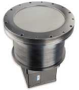
FIGURE 2. Fiber tapers, enclosed in the cone-shaped extension on the sensor house, are doped with heavy metals such as terbium to reduce the impact of stray x-ray radiation on the silicon sensor beneath, while providing increased magnification for x-ray inspection systems.
By engineering visible sensors to harden these components against destructive x-ray radiation, expanding the variety of x-ray sources to provide low-cost x-ray photons from 1-keV (~0.1-nm) tubes through linear accelerators capable of producing megaelectronvolt x-rays, and combining the result with proven image-processing system design and software, the machine-vision industry is adapting the technology of medical science to an industrial inspection tool capable of seeing through nearly any material to find hidden defects. As sources continue to develop for fast-risetime, pulse x-rays capable of producing more x-ray photons than the standard tungsten-electron beam interaction of today's conventional sources, x-ray AOI systems will improve in throughput, safety, and resolution.
X-ray system reveals electronics' hidden flaws
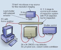
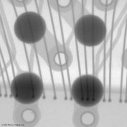
Ball-grid-array (BGA) or column-grid-array chip-scale package inspection is an ideal application for an x-ray automated optical inspection (AOI) system because defects between chip connection pads, solder balls, and PCB wire traces are all hidden underneath the chip. Standard BGA x-ray inspection systems use 2000 × 2000-pixel or greater CMOS or CCD array sensors with an integrated phosphor scintillator because these applications typically require spatial resolution of a few microns to identify defects common to BGA connections, such as bridges and missing solder balls (see figure below).
Object under test can be placed perpendicular to the optical axis if only 2-D image information is required, or off-axis for 3-D data. Full 3-D data sets require a computed-tomography approach. Platinum or other metals are used in lower-energy shutter systems, but for systems above 60 keV, lead is the most cost-effective material.
Compounding the spatial-resolution challenge are the physics behind x-ray photons. X-rays tend to pass directly through most materials or be absorbed, rather than refracting through materials with different optical properties, as visible photons do. Therefore, x-ray systems are limited to small magnifications, typically operating at 1X or no magnification, with inspection areas approximately the same size as the sensor (a few inches or less, depending on sensor size). CMOS and CCD sensors offer the smallest pixel sizes and, therefore, the best spatial resolution for an x-ray imaging system.
To increase the sharpness of the final image, BGA inspection systems typically use a microfocus x-ray source with a 20-µm or smaller aperture. These sources provide peak photon energies at half-maximum power operation of between 70 and 90 keV for excellent transmission through the plastic and metal object under inspection, while reducing "blur" around objects. The size of the blurred edge is relative to the size of the x-ray aperture.
Because these sources operate at energies above soft-x-ray levels (approximately 10 keV), silicon-based detectors use a terbium or other heavy-metal-doped fiber faceplate located between the scintillator and sensor to block stray x-rays that are not absorbed by the scintillator screen. This arrangement keeps the x-rays from damaging the sensor over time and increasing the sensor's dark current, according to David Litwiller, vice president of marketing and business development for Dalsa. Fiber faceplates, opposed to tapered fiber plates, are also less expensive than tapered fiber arrays, which offer single-digit magnifications at the expense of sharpness to the x-ray image, but can be used to inspect a larger area on the BGA than the sensor size, or obtain greater magnification of a particular region of interest (see photo on p. 24).
X-ray image reveals a ball grid array with wirebonds.
Microfocus x-ray sources can take several minutes to "warm up," prompting users to operate the sources continuously rather than pulsing or cycling the illumination source. The small aperture size requires scanning the object of interest across the optical axis for 100% inspection. To avoid blurring of the image due to part movement during sensor readout and to increase throughput, BGA inspection systems include a mechanical shutter that is open during acquisition time and closed during sensor readout.
Typically, shutter-actuation speed, even with lead shutters, is not a problem for microfocus-sized apertures. When heavy metals, such as lead or platinum iridium, are used in larger apertures, faster shutter speeds are achieved by using two blades that meet in the middle of the aperture rather than a single shutter blade, according to Stephen Pasquarella, product manager at Vincent Associates.
The shutter control electronics can be triggered by either the frame grabber or cameras with built-in alarm-signaling capabilities, where the shutter control signal is based on the beginning and end of the sensor readout cycle. "Even saving a couple hundred milliseconds is important to the electronics industry," notes John Gilmore, product manager for flat-panel silicon detectors at Hamamatsu.
Image data are fed from the sensor to the frame grabber. Although x-ray systems typically use multimegapixel sensors because of the small defect size common to electronics inspection and the difficulty of magnifying x-ray systems while maintaining image sharpness, the long acquisition times for an x-ray sensor (upward of 1 s) due to limited x-ray photon availability from conventional x-ray sources means that the system does not require exceptional memory buffers common to high-speed or real-time inspection systems.
X-ray images are typically preprocessed to correct for column breaks and defective pixels, tiling of smaller sensor blocks into megapixel blocks, or defects in the scintillator or optical fibers. BGA inspection systems then use edge detection or search algorithms to identify specific items, such as the solder ball connection to the BGA pad, and blob analysis to identify bridges, under solder, over solder, and other defects common to BGA connections.
— R.W.H.
Company Info
Dalsa Waterloo, ON, Canada www.dalsa.com
Hamamatsu Bridgewater, NJ, USA www.hamamatsu.com
Oxford Instruments America Concord, MA, USA www.oxinst-instruments.com
Rad-icon Imaging Santa Clara, CA, USA www.rad-icon.com
Vincent Associates Rochester, NY, USA www.uniblitz.com


