CMOS single-chip sensor captures 3-D images
In many applications such as vision-guided robotics, it is necessary to accurately locate three-dimensional (3-D) objects. If an ordinary camera is used in such applications, objects of different shapes and sizes can appear the same, and distance and shape cannot be computed. To overcome these limitations, systems designers often take a number of measurements of objects with multiple ordinary cameras (for example, stereoscopic cameras) and mathematically compute the shape or distance. Alternatively, laser scanners can be used. While stereoscopic cameras require precise calibration, alignment, and substantial computation, laser-based systems are usually more expensive and require rapidly moving parts.
To address these issues, Canesta (San Jose, CA, USA; www. www.canesta.com) has recently patented electronic perception technology, a CMOS-based single-chip imaging technology that creates 3-D images of nearby objects in real time. This technology, first shown at The Vision Show East (May 2004; Boston, MA,USA), uses a time-of-flight principle to determine the distance from each pixel in the array to the corresponding feature in the scene. The time of flight is measured by detecting the phase difference between a modulated light source (an array of laser diodes or LEDs near the sensor) and the returning light at every pixel in every frame.
"If the transmitted light is modeled as a sinusoid," says Jim Spare, Canesta vice president of product marketing, then it can be represented as A0 sin (ωt). "The reflected light then returns to the image sensor with a phase delay, φ, and thus may be represented as A1 sin (ωt-φ)."
null
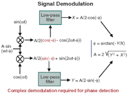
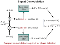
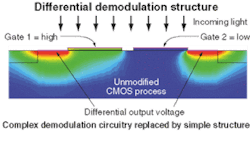
Prototype 3-D vision sensor from Canesta measures the distance of objects from sensor-reflected time-of-flight signals that are usualy modulated mathematically (top). In the CMOS device, the mathematics are embodied in a switched differential demodulation structure, where the differential output voltage of switched photodiode gates can be used to determine depth (bottom). Results can then be color coded for visualization purposes.
To compute the distance of each object from the sensor, the phase, φ, must first be determined. As the phase directly relates to the distance from the object to the camera (φ = 2dω/c), computing the phase will lead to a distance measurement. It is theoretically possible to determine this time-of-flight measurement mathematically through a process of demodulation by combining two reference signals with the returning light signal (see figure). However, digital or analog circuitry to perform this calculation would be too expensive and bulky to implement practically in a CMOS chip.
"Rather than compute this mathematically," says Spare, "Canesta invented a way to leverage the properties of the CMOS silicon semiconductor material to do this demodulation automatically at every pixel. The distance value is provided right out of the hardware and does not require expensive signal or image processing to generate the distance value. Canesta's current image sensor consists of a 64 × 64 array of light-sensitive elements (pixels), each of which consists of two gates.
To determine the phase delay of the incoming light, each gate is alternately switched in synchronization with the modulation frequency of the emitted light from the light source. While one of the gates is switched in phase with the frequency of light from the photodiode array, the other is switched out of phase. In this way, a charge will build at each gate, proportional to the amount of light received during that period. Effectively, this CMOS silicon structure has performed the signal demodulation. Thus, the differential output voltage between the two gates provides an effective measure of the phase shift of the light and the distance the object is away from the sensor.
In this way, each of the dual-gate pixels can provide a range value (which in Canesta's demo is color-coded for easy visualization). The chip, designed by Canesta, is built in a standard 0.25-µm CMOS process at United Microelectronics (Hsinchu, Taiwan). An evaluation system that includes the CMOS IC, lens, light source, and evaluation software will be available in August. Chips will be available for OEM camera and system vendors in sample quantities by the end of the year. At present, the sensor has a depth resolution of 1 cm/pixel/frame and a 64 × 64-pixel array. Spare expects further developments to include an increased depth resolution of 1 mm, larger array sizes, and possibly a color depth sensor.


