FPGAs push PC parallel-processing power
Incorporating dense, high-performance FPGAs onto frame grabbers and image processors, vendors are increasing image-processing throughput.
By Andrew Wilson, Editor
Despite the increase in processing power of off-the-shelf CPUs, image-processing software used in machine-vision applications often demands algorithms that are accelerated by RISC, DSP, or field-programmable gate arrays (FPGAs). Because such algorithms are often parallel in nature, dataflow architectures built around these devices are frequently used to off-load the host PC in computationally intensive functions such as filtering, color correction, template matching, and noise suppression.
“Because of the comparatively small size of the image-processing market, most special-purpose image processors have been unable to keep pace with advances in general-purpose processors,” says Bruce A. Draper, associate professor at Colorado State University. “As a result, developers who adopt them are often left with obsolete technology. FPGAs, on the other hand, enjoy a multibillion-dollar market as low-cost ASIC replacements. Consequently, increases in FPGA speeds and capacities have followed or exceeded Moore’s law for the last several years, and developers can continue to expect them to keep pace with general-purpose processors,” he says.
FPGA FAMILIES
Two companies currently dominate the FPGA marketplace-Xilinx, with its Virtex family, and Altera, with its Stratix series of devices. In choosing a specific family for image-processing applications, designers of frame grabbers must consider a number of factors. In addition to being dependent on the embedded image-processing algorithms used in the FPGA, there are many factors that can affect how each device performs, including algorithm partitioning, the use of on-board DSP blocks such as multipliers and adders, phase-lock loops, I/O elements, and the number and types of RAM blocks.
Both Altera and Xilinx offer intellectual-predefined and tested software modules (or cores) that board vendors can use to create system functions using FPGAs. Both companies offer, for example, shift registers, multipliers, FIR filters, and DCT cores, as well as memory controllers, bus interfaces, and embedded DSP cores. By implementing these cores, board vendors can bring product to market rapidly while offering added image-processing functions accelerated in FPGA hardware. Because of the flexibility inherent in FPGAs, image-processing functions that can be implemented range from simple algorithms, such as capturing a region of interest and edge detection (comparing the incoming pixels to a certain threshold level), to complex system implementations including filters that perform convolutions on the incoming pixel data, DCTs, FFTs and warping functions.
ON-BOARD ARRAYS
Most current frame grabbers and image processors use FPGAs. How they are implemented in these designs, however, differentiates the boards, the intended customers, and the embedded systems they target. To reduce the cost of the glue logic once associated with such products, some frame-grabber vendors implement simple functions such as camera control, triggering, I/O set-up functions, and PCI-based interfaces using FPGAs.
In these designs, systems integrators are not encouraged or even allowed access to the programmable nature of the board. Supplied with both analog- and digital-camera interfaces, these boards are often shipped with a specific camera-configuration file or set of configuration files that allow the systems integrator to match the board to a specific camera. In choosing a camera for simple image acquisition, developers should check with each board manufacturer to determine which camera-configuration files are supported.
In other cases, however, the distinction of which functions are performed with on-board FPGAs is not as obvious. Given the flexibility of FPGA devices, manufacturers often cram multiple functionality into these devices, including image-processing functions such as matrix multiplication for high-speed filtering and color correction, as well as PCI interfaces and DMA bus-mastering functions.
ADDED FUNCTIONS
Because FPGAs do offer flexibility, many vendors have implemented specific functions such as color-space conversion directly on FPGAs. These predefined functions can then be accessed though callable libraries or high-level machine-vision or image-processing packages, where required. Once again, the number and types of functions are vendor-specific, and developers wishing to rapidly deploy specific algorithms should initially check whether the algorithms they may require have already been embedded into hardware.
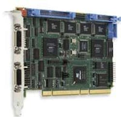
In the past, frame grabbers offered without an on-board processor were referred to as “dumb.” However, by implementing on-board FPGAs, the distinction between what was once called a frame grabber (without an on-board processor) and an image-processing board (with processing capability) is now blurring. Featuring a single or dual Camera Link camera interface configuration, the R64-CL-IP2 from Bitflow is a good example (see Fig. 1).
In the single-camera configuration, the R64-CL-IP2 is capable of supporting a Base, Medium, or Full Camera Link camera. Output configurations include two taps, three taps (RGB), four taps, and eight taps. The dual-camera-configuration R64-CL can support two identical Base Camera Link cameras. By using an FPGA on the board, the Bitflow R64-PCI-CL-IP2 features real-time Bayer-filter interpolation using the company’s BayView application, offered as part of its software-development kit.
CUSTOMIZED BOARDS
Programming FPGAs to perform specific functions usually requires intimate knowledge of very-high-speed IC hardware description language (VHDL). Realizing this, many board vendors offer the capability to add additional FPGA power onto their boards with optional FPGA mezzanine modules. Vendors often mandate that they perform customization of such devices, however, because they realize the complexity of their own specific architecture and FPGA capability.
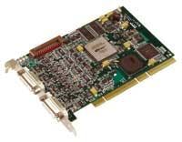
For applications that require some processing acceleration or the off-loading of some processing tasks from the host CPU, the Solios XA from Matrox Imaging is available with a configurable FPGA-based processing core. This optional processing core is based on the Altera Stratix family of pin-compatible FPGA devices and can include DDR SDRAM and a QDR SRAM. Data to and from the processing core travels over the on-board secondary PCI-X bus and/or a dual-simplex link to the video capture controller (see Fig. 2).
The processing core is intended for operations such as per-pixel gain and offset (flat-field) correction, look-up table, or filter, and must be customized by Matrox Imaging. In addition to acquiring data from up to four single-output video sources, inputs can be combined to acquire images from two dual-output video sources or one RGB video source.
INSIDE THE CODE
While some manufacturers shy away from encouraging developers to program on-board FPGAs, others actively encourage it. Building products specifically tailored for high-performance systems, these companies argue that to truly tailor FPGA-based systems for high performance requires real-time operating systems (RTOSs) tailored with FPGA design environments and FPGA-specific software tools.
By offering such products, vendors realize that although development times may be longer, system performance will be dramatically increased. Because of this, however, they are not trying to sell single-board-level products. Rather, they are trying to work with sophisticated OEMs who require multiple products over a number of years.
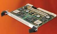
Recently, SBS Technologies strengthened its product offerings in this area with the Tsunami 6U CPCI A80, an FPGA-based board also based on the Stratix family (see Fig. 3). Using two Altera Stratix EP1S80 FPGA devices, the board features dual PMC slots for I/O connectivity and a direct 1-Gbyte/s path from the PMC slots to the P4 connector on the FPGA devices. To support the board, SBS supplies its SBS Wave FPGA software tool kit and Altera’s Quartus II software design environment. The Tsunami 6U CPCI supports the Green Hills Integrity RTOS and Linux and Windows XP/2000.
DRAG AND DROP
For the systems integrator wishing to tweak the maximum performance from an FPGA frame grabber or image processor, the thought of VHDL design environments and development tools may appear daunting. Indeed, this is something that has not gone unnoticed by board vendors wishing to promote FPGA products. For a number of years, many universities and companies have sought to bring pipelined image processing to broader markets by developing easy-to-use graphical-based tools that offer flexibility while at the same time do not requiring sophisticated VHDL programming. Luckily, such tools are now emerging.
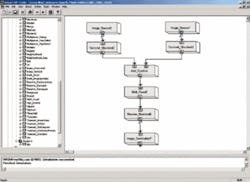
Visual CHIP Studio (VCS) from Datacube, for example, is a graphical FPGA programming tool with which developers can define, verify, and simulate the contents of the FPGA and subsequently control it in a video-layered-library framework. As a graphical tool for FPGA programming, VCS provides an interactive design and development environment from which designers can create image-processing systems.
FIGURE 4. Datacube Alpha Blend is a Visual CHIP Studio project file that blends two images together (top). The data flow is from top to bottom, where two image sources are added together, shifted to normalize the result, and the result placed into an image-destination buffer. The operation of the algorithm can be simulated by assigning an image file to each image source and testing with probe points. The probe points are the three “magnifying glasses”-one on each image source and one just prior to the image destination (bottom).
Using drag-and-drop operators, VCS permits algorithmic building blocks or operators to be connected to create image-processing pipelines that operate at 100 MHz (see Fig. 4). VCS operators are software representations of FPGA image-processing functions. Using these operators allows simple pipelines or composite image-processing operators to be assembled from standard operators. Once completed, verified, and simulated, an FPGA bitstream can control the FPGA on Datacube’s MaxRevolution PC-based image-processing hardware.
According to In-Stat/MDR, the market for FPGAs increased from $2.9 million in 2001 and will reach$603.1 million by 2006. In most cases low-level FPGA functionality will be hidden from the systems developer, but the benefits of reusable IP and rapid reconfigurability will lead to increased performance and reduced manufacturing costs.
Company Info
Altera, San Jose, CA, USA www.altera.com
Basler Vision Components, Ahrensburg, Germany www.baslerweb.com
Bitflow, Woburn, MA, USA www.bitflow.com
Colorado State University, Fort Collins, CO, USA www.cs.colostate.edu
Datacube, Danvers, MA, USA www.datacube.com
Eltec Electronik, Mainz, Germany www.eltec.de
Epix, Buffalo Grove, IL, USA www.epix.com
In-Stat/MDR, Scottsdale AZ, USA www.instat.com
Matrox Imaging, Dorval, QC, USA www.matrox.com/imaging
National Instruments, Austin, TX, USA www.ni.com
Redlake, San Diego, CA, USA www.redlake.com
SBS Technologies, Albuquerque, NM, USA www.sbs.com
Xilinx, San Jose, CA, USA www.xilinx.com
PCI Express frame grabber shown at NI Week
At NI Week (Aug 17-19, 2004), National Instruments showed the world’s first frame grabber built around the PCI Express standard (see Vision Systems Design, May 2004, p. D7). According to Kyle Voosen, NI machine-vision product manager, the PCIe-1429 product will be officially announced in September. Headlining a keynote speech at the show, the board was also featured on the exhibition floor, where it was shown interfaced to the 1280 * 1024-pixel, 500-frames/s A504k Camera Link camera from Basler Vision Components.
In a high-speed imaging demo, the board captured 1.2-Mpixel images of a bursting water balloon over the PCI Express interface. “While we have seen this demo performed on stand-alone imaging systems, such as MotionMeter from Redlake, this is the first time it has been demonstrated over PCI Express,” says Voosen.
NI also announced new versions of its Vision Development Module (VDM) and Vision Builder for Automated Inspection. “NI’s VDM combines the company’s OCR toolkit, Vision Assistant, libraries for LabVIEW, libraries for text-based ADEs, and several new algorithms,” says Voosen. New algorithms include geometric matching, 2-D barcode readers, classification tools, and C-code generation.
Vision Builder for Automated Inspection is a configuration environment for nonprogrammers used to build applications with the Compact Vision System. New features include built-in industrial communication protocols, color matching, and a calculator tool for performing arithmetic and logic operations on multiple measurements from multiple cameras.
“Whereas PCI-X is meant for server-class machines and workstations, PCI Express is multisegmented and will encompass the spectrum of machines from desktop PCs to workstations to servers,” says Laval Tremblay, director of engineering at Matrox Imaging. In a recent interview for the company’s Imaging Insight newsletter, Tremblay said that Matrox will support the PCI Express bus on its existing frame grabbers relatively soon.
“PCI Express has multiple benefits for the user,” he adds. “For example, the minimum speed of PCI Express is almost twice the speed of the PCI bus. PCI Express is less expensive to implement, so costs will be reduced for the connectors. Because it is a serial instead of parallel bus, there are savings in terms of the number of pins, and it’s not as difficult to design the boards.
But it’s not just NI and Matrox that plan PCI Express frame grabbers and image processors. Other manufacturers readying PCI Express boards include Epix, Bitflow, and Eltec Electronik.
According to Chuck Petersen, president of Epix, the company is planning a dual Base Camera Link frame grabber board for a 4x PCI Express implementation for introduction in November. Bitflow will also offer a frame grabber board later this year. According to Bill Carson, the R64 Express board will be developed around the company’s R64-PCI-CL and will support Base, Medium, Full, or Dual Base Camera Link camera configurations. Developed around Intel’s PCI-to-PCI Express bridge chip, the board will feature 4x PCI Express bus performance of around 1 Gbybte/s (up from 390 Mbytes/s on the 64-bit/66-MHz PCI bus with an Intel 7500 series motherboard chipset) and up to 528-Mbyte/s camera data-input capability.
Eltec Elektronik’s frame grabber, the p3i_ASYNC PCI Express, will feature four simultaneous asynchronous input channels and can replace up to four monochrome frame-grabber boards for the acquisition of four independent camera signals at 25 MHz/8 bit using four independent ADCs. Parallel acquisition into main memory and graphics memory is supported through DMA. The frame grabber supports the 1x PCI Express interface with twice the data rate of the 32-bit PCI bus and runs under Windows NT/2000/XP and Linux.
-A. W.
