CPU or FPGA for image processing: Which is best?
As multicore CPUs and powerful FPGAs proliferate, vision system designers need to understand the benefits and trade-offs of using these processing elements.
Brandon Treece
Machine vision has long been used in industrial automation systems to improve production quality and throughput by replacing manual inspection traditionally conducted by humans. We've all witnessed the mass proliferation of cameras in our daily lives in computers, mobile devices, and automobiles, but the biggest advancement in machine vision has been processing power. With processor performance doubling every two years and a continued focus on parallel processing technologies like multicore CPUs and FPGAs, vision system designers can now apply highly sophisticated algorithms to visualize data and create more intelligent systems.
This increase in performance means designers can achieve higher data throughput to conduct faster image acquisition, use higher resolution sensors, and take full advantage of some of the latest cameras on the market that offer the highest dynamic ranges. An increase in performance helps designers not only acquire images faster but also process them faster. Preprocessing algorithms such as thresholding and filtering or processing algorithms such as pattern matching can execute much more quickly. This ultimately gives designers the ability to make decisions based on visual data faster than ever.
As more vision systems that include the latest generations of multicore CPUs and powerful FPGAs reach the market, vision system designers need to understand the benefits and trade-offs of using these processing elements. They need to know not only the right algorithms to use on the right target but also the best architectures to serve as the foundations of their designs.
Inline vs. co-processing
Before investigating which types of algorithms are best suited for each processing element, you should understand which types of architectures are best suited for each application. When developing a vision system based on the heterogeneous architecture of a CPU and an FPGA, you need to consider two main use cases: inline and co-processing. With FPGA co-processing, the FPGA and CPU work together to share the processing load. This architecture is most commonly used with GigE Vision and USB3 Vision cameras because their acquisition logic is best implemented using a CPU. You acquire the image using the CPU and then send it to the FPGA via direct memory access (DMA) so the FPGA can perform operations such as filtering or color plane extraction. Then you can send the image back to the CPU for more advanced operations such as optical character recognition (OCR) or pattern matching. In some cases, you can implement all of the processing steps on the FPGA and send only the processing results back to the CPU. This allows the CPU to devote more resources to other operations such as motion control, network communication, and image display.
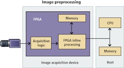
In an inline FPGA processing architecture, you connect the camera interface directly to the pins of the FPGA so the pixels are passed directly to the FPGA as you send them from the camera. This architecture is commonly used with Camera Link cameras because their acquisition logic is easily implemented using the digital circuitry on the FPGA. This architecture has two main benefits. First, just like with co-processing, you can use inline processing to move some of the work from the CPU to the FPGA by performing preprocessing functions on the FPGA. For example, you can use the FPGA for high-speed preprocessing functions such as filtering or thresholding before sending pixels to the CPU. This also reduces the amount of data that the CPU must process because it implements logic to only capture the pixels from regions of interest, which increases overall system throughput. The second benefit of this architecture is that it allows for high-speed control operations to occur directly within the FPGA without using the CPU. FPGAs are ideal for control applications because they can run extremely fast, highly deterministic loop rates. An example of this is high-speed sorting during which the FPGA sends pulses to an actuator that then ejects or sorts parts as they pass by.
CPU vs. FPGA vision algorithms
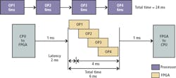
With a basic understanding of the different ways to architect heterogeneous vision systems, you can look at the best algorithms to run on the FPGA. First, you should understand how CPUs and FPGAs operate. To illustrate this concept, consider a theoretical algorithm that performs four different operations on an image and examine how each of these operations runs when implemented on a CPU and an FPGA.
CPUs perform operations in sequence, so the first operation must run on the entire image before the second one can start. In this example, assume that each step in the algorithm takes 6 ms to run on the CPU; therefore, the total processing time is 24 ms. Now consider the same algorithm running on the FPGA. Since FPGAs are massively parallel in nature, each of the four operations in this algorithm can operate on different pixels in the image at the same time. This means the amount of time to receive the first processed pixel is just 2 ms and the amount of time to process the entire image is 4 ms, which results in a total processing time of 6 ms. This is significantly faster than the CPU implementation. Even if you use an FPGA co-processing architecture and transfer the image to and from the CPU, the overall processing time including the transfer time is still much shorter than using the CPU alone.
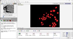
Now consider a real-world example for which you are preparing an image for particle counting. First, you apply a convolution filter to sharpen the image. Next, you run the image through a threshold to produce a binary image. This not only reduces the amount of data in the image by converting it from 8-bit monochrome to binary, but also prepares the image for binary morphology. The last step is to use morphology to apply the close function. This removes any holes in the binary particles.
If you execute this algorithm only on the CPU, it has to complete the convolution step on the entire image before the threshold step can begin and so on. This takes 166.7 ms when using the NI Vision Development Module for LabVIEW and the cRIO-9068 CompactRIO Controller based on a Xilinx Zynq-7020 All Programmable SoC. However, if you run this same algorithm on the FPGA, you can execute every step in parallel as each pixel completes the previous step.
Running the same algorithm on the FPGA takes only 8 ms to complete. Keep in mind that the 8 ms includes the DMA transfer time to send the image from the CPU to the FPGA, as well as time for the algorithm to complete. In some applications, you may need to send the processed image back to the CPU for use in other parts of the application. Factoring in time for that, this entire process takes only 8.5 ms. In total, the FPGA can execute this algorithm nearly 20 times faster than the CPU.
So why not run every algorithm on the FPGA? Though the FPGA has benefits for vision processing over CPUs, those benefits come with trade-offs. For example, consider the raw clock rates of a CPU versus an FPGA. FPGA clock rates are on the order of 100 MHz to 200 MHz. These rates are significantly lower than those of a CPU, which can easily run at 3 GHz or more. Therefore, if an application requires an image processing algorithm that must run iteratively and cannot take advantage of the parallelism of an FPGA, a CPU can process it faster. The previously discussed example algorithm sees a 20X improvement by running on the FPGA. Each of the processing steps in this algorithm operates on individual pixels, or small groups of pixels, at the same time, so the algorithm can take advantage of the massive parallelism of the FPGA to process the images. However, if the algorithm uses processing steps such as pattern matching and OCR, which require the entire image to be analyzed at once, the FPGA struggles to outperform. This is due to the lack of parallelization of the processing step as well as the large amount of memory required to analyze the image versus a template. Though FPGAs have direct access to internal and sometimes external memory, it is usually nowhere near the amount of memory available to a CPU or the amount needed for these processing operations.
Overcoming programming complexity
The advantages of an FPGA for image processing depend on each use case, including the specific algorithms applied, latency or jitter requirements, I/O synchronization, and power utilization.
Often using an architecture featuring both an FPGA and a CPU presents the best of both worlds and provides a competitive advantage in terms of performance, cost, and reliability. Unfortunately, one of the biggest challenges to implementing an FPGA-based vision system is overcoming the programming complexity of FPGAs. Vision algorithm development is, by its very nature, an iterative process. You know up front that you have to try a few approaches with any task. Most of the time, you need to determine not which approach works, but which approach works best, and "best" is different from application to application. For some applications, speed is paramount. In others, it's accuracy. At a minimum, you need to try a few different approaches to find the best one for any specific application.
To maximize productivity, you need to get immediate feedback and benchmarking information on your algorithms regardless of the processing platform you are using. Seeing algorithm results in real time is a huge time-saver when you are using an iterative exploratory approach.
What is the right threshold value? How big or small are the particles to reject with a binary morphology filter? Which image preprocessing algorithm and algorithm parameters can best clean up an image? These are all common questions when developing a vision algorithm, and having the ability to make changes and see the results quickly is key. However, the traditional approach to FPGA development can slow down innovation due to the compilation times required between each design change of the algorithm.
One way to overcome this is to use an algorithm development tool that helps you develop for both CPUs and FPGAs from the same environment while not getting bogged down in FPGA compilation times. The NI Vision Assistant is an algorithm engineering tool that simplifies vision system design by helping you develop algorithms for deployment on either the CPU or FPGA. You also can use the Vision Assistant to test the algorithm before compiling and running it on the target hardware while easily accessing throughput and resource utilization information.
Brandon Treece, Senior Product Marketing Manager, National Instruments, Austin, TX, USA (www.ni.com).
Related stories:
International Vision Standards Meeting 2019 further develops camera interface standardization
Smart cameras evolve to meet expanding machine vision needs
Neural network standard streamlines machine learning tech development
Share your vision-related news by contacting Dennis Scimeca, Associate Editor, Vision Systems Design
SUBSCRIBE TO OUR NEWSLETTERS


