Deep learning software enhances PCB inspection system
Automated optical inspection (AOI) is an automated visual inspection technique involving the scanning of the surface of a printed circuit board (PCB) to acquire a clear image. AOI systems can check for defects, including short circuits, excessive or insufficient copper, open circuits, nicks, burrs, copper slags, missing components, and deflections.
Because of the number of surface defects that exist, the inspection of PCBs can be more difficult compared with that of general electronic components, and oftentimes requires a second manual screening to differentiate between real defects and false-positives before the PCB returns to the product line.
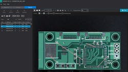
Designed by G4 Technology Co., Ltd. (Taipei City, Taiwan; https://www.g4.com.tw), the AI Defect Inspection System leverages machine vision cameras and deep learning software to accurately inspect, detect, mark, and classify PCB defects. Compared with traditional machine vision techniques, this system can reportedly analyze complex images, improve image interpretation skill and the accuracy of automatic visual inspection, and conduct automatic classification of defects.
The vision system consists of a camera from Allied Vision (Stadtroda, Germany; www.alliedvision.com), a Fujifilm (Tokyo, Japan; www.fujifilm.com) high-resolution lens, and SuaKIT deep learning software from SUALAB (Seoul, South Korea; www.sualab.com). The camera in the system, a Manta G-032C model, is based on the 0.3 MPixel Sony ICX424 color CCD sensor, which has a 7.4 µm pixel size and reaches a frame rate of 80.7 fps at full resolution.
This camera, according to Ken Chou, G4 Technology General Manager, was selected because of its frame rate capability and its match with the AI inspection algorithm, due to the quality and stability of the camera.
In deep learning software, example-based algorithms are trained with images of both acceptable and unacceptable products, unlike rule-based algorithms that require manual setting of defect criteria. SuaKIT inspects defect areas by analyzing various defects on products (segmentation), classifying images and categorizing them into defect types (classification), and detecting each target object in an image by class (detection).
To do so, SuaKIT’s algorithm is taught with approximately 100 images of normal and defective products, establishing a neural network in about 15 minutes’ time. After this, 80 images per second can be collected and processed on a production line as a result of the camera’s frame rate, allowing the software to automatically learn and analyze defect criteria and differentiate between normal and defective object images.
Required image data during the initial stage of the deep learning algorithm varies with the complexity of the images. Generally, 50 to 100 images are required, which allows the system to handle customer-specific defect standards. Implementing deep learning software replaces the need for human visual inspection in such cases, allowing for the relocation or deployment of people to other manufacturing processes or tasks at a facility, thus improving overall productivity.
The software does not require instance-by-instance coding but operates through self-learning by gathering and entering data on defects, according to SUALAB. The software is also designed so that through CUDA (Compute Unified Device Architecture) technology, data can be processed at high speed through a GPU.
In a similar application in which SuaKIT was deployed (bit.ly/VSD-SUA), the identification of defective PCB products using conventional machine vision inspection methods, i.e. pattern matching algorithms, resulted in accuracy below 40%. The over-detection rate was also high, requiring at least three manual inspectors in the process, even after automated inspection was done. SuaKIT, according to Hanjun Kim, former Global Business Manager, improved accuracy to 97.4% in this application.
About the Author

James Carroll
Former VSD Editor James Carroll joined the team 2013. Carroll covered machine vision and imaging from numerous angles, including application stories, industry news, market updates, and new products. In addition to writing and editing articles, Carroll managed the Innovators Awards program and webcasts.
