Integrated system performs semiconductor inspection of scribed wafers
Integrated system performs semiconductor inspection of scribed wafers
Optical-character-recognition subsystem helps speed robotic wafer fabrication by automatically validating laser-scribed data.
By Lawrence J. Curran, Contributing Editor
In semiconductor fabrication, wafer alignment and identification usually require two successive assembly steps because the equipment--a prealigner to position the wafer and an optical-character-recognition (OCR) unit to read laser-scribed ID data--has been too bulky to fit in a small subsystem. To overcome this
problem, three system integrators have combined their expertise to interface the hardware and software needed to perform both functions at one station. In addition, the station can capture and validate an image of the laser-scribed identification marks on the wafer`s opaque nonreflective surface.
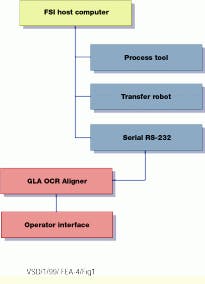
The system integrators are GL Automation Inc. (GLA; Dallas, TX), Acutec Inc. (Portland, OR), and FSI International Inc. (Allen, TX). Acutec is an OEM supplier of Cognex Corp. (Natick, MA) OCR components used for the wafer ID process. GLA integrates these and other elements with its wafer prealigner and, in turn, furnishes an optical subsystem to FSI for integration into a computer-based, robotic wafer-handling and control system (see Fig. 1).
Their development efforts are expected to save wafer-processing time, decrease cost, and increase throughput. In addition, the OCR subsystem will automatically identify all products as they pass through the system and will reduce the wafer`s exposure to potential damage from excessive handling.
Galle Lin, GLA president, says his company`s task, as defined by FSI, was to develop a self-contained wafer prealigner with an integrated backside OCR subsystem. Size constraints were a major design challenge because the prealigner/optical subsystem had to fit within one station of a new, proprietary FSI processing tool, which had to operate as a slave to the wafer-handling control system.
For more than a year, GLA and FSI designers worked together to integrate prealignment technology with wafer-identification processes. "Our personal relationships with FSI management and our experience in developing products for Texas Instruments and other semiconductor manufacturers well-positioned GLA as the supplier for this project," says Lin.
Prealign and identify
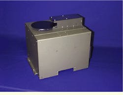
The GLA-furnished optical subsystem has three major hardware blocks and two main software elements. The key hardware components are the GLA-built wafer prealigner, a personal computer, and an optical subsystem (see Fig. 2). The software comprises the aligner/communications package and the Cognex OCR application software. "The mechanical challenges we faced included how to package the hardware components into the smallest package possible and how to design and produce an optical subsystem to capture the image of a laser mark on an opaque nonreflective surface," Lin reports.
The optical subsystem is connected to an FSI host computer, which initiates all operations, including those of a robot that feeds the wafers to the prealigner. Upon receiving a request from the host, the optical subsystem acknowledges the request and then carries out the align and identify functions. After these operations are completed, the robot removes the wafer from the prealigner, and the cycle repeats.
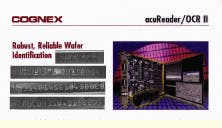
Key technology from Cognex controls system illumination and also identifies the custom font of the laser-scribed wafer ID data. "The algorithms and flexibility of the Cognex software provide the power to read many customers` products," says Jeff Friedman, president of Acutec. A standard font library and custom fonts are available to use within the reading application.
The Cognex hardware platform, a half-size model 6140 PCI card, "allowed us to keep the package small," Lin says. "We chose a passive backplane and a single-board Pentium PC running Windows 98 to support the reading and alignment operations because of the PC`s small footprint and high performance," he adds.
The optical subsystem contains a built-in CCD camera from Philips Professional Imaging (Breda, Netherlands), an autoswitching power supply, a hard drive, and additional electronics to support the alignment operation and the external input/output circuits.
The image acquisition and the illumination control provided with the Cognex product "solved the identification applications. By offering both camera sync and phase-locked loop circuits, we evolved a simple acquisition strategy," Lin says. A GLA-designed custom LED illuminator uses a fixed-focal-length lens and is driven by standard software. To embed the optical subsystem within the prealigner, GLA folded the optical path to achieve a restricted working distance dictated by the machine height of approximately 6 in.
"Our illuminator can provide both bright-field and dark-field illumination and is fully compliant with the Cognex software to automatically switch illumination modes and intensity under program control," Lin says.
How it works
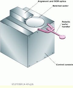
During the alignment operation, the robot presents wafers to the optical subsystem and removes them automatically. The prealigner, when signaled, performs alignment, optical character recognition of the scribed data, and re-orientation upon request (see Fig. 3).
Independent messages are initiated by the FSI host, with each serial RS-232 command being serviced by the prealigner software. Each message is acknowledged and acted upon. After message completion, the aligner issues a "Done" command and then sends back data, if requested.
In system operation, wafers are placed on a vacuum chuck, and the host sends a "Begin Alignment" message. Then, the prealigner turns on the vacuum equipment and begins the alignment operation. The wafer is rotated up to 360 to find its notch. Next, the prealigner software returns the incoming wafer data, along with its position and notch location, to the FSI host system, which then sends a "Read" message to the prealigner. The prealigner, in turn, rotates the wafer to position the previously laser-scribed data in a reading window for the CCD camera. After this repositioning is completed, the Cognex-controlled OCR unit reads the scribe.
If the reading is successful, the prealigner sends the scribed serial number back to the host, which then performs a checksum calculation to validate the scribe and the completeness of the transmission. If the scribe is obscured or difficult to read, the reading software can automatically readjust the illumination and image-processing filters to re-read the scribe. "Here, the Cognex 6140 board, with its on-board DSP, quickly tunes the system to read noisy images," Friedman says. "Reading speeds of 250 ms are typical, allowing the system to try many reading settings and filters to correctly identify the scribe," he adds.
After the scribe reading is completed, the wafer is returned to a final orientation position. The prealigner then sends a "Complete" message to the FSI host, which dispatches the robot to remove the wafer. After the robot is in position, the host signals the prealigner to release the vacuum and confirm the request. Upon vacuum-release acknowledgment, the robot removes the wafer from the vacuum chuck, thereby completing the inspection cycle.
Lin says GLA`s prior experience in designing wafer prealigners, along with "a key relationship with Acutec, provided us with tools and resources to accurately identify many end-user products for consideration. Although these technologies were never previously tied together in a small package, we felt we had a winning combination to solve the challenges presented by this application," he says.
FIGURE 1. The wafer-handling optical subsystem hardware comprises a wafer prealigner, a personal computer, and an optical subsystem. The software comprises an aligner/ communications package and OCR application software. The optical subsystem is connected to a host computer, which initiates all operations, including those of a robot that feeds the wafers to the prealigner. Controlled illumination helps to identify the custom font of the laser-scribed wafer identification data.
FIGURE 2. The optical subsystem contains a built-in CCD camera, an auto-switching power supply, a hard drive, and additional electronics to support the alignment operation and the external input/output circuits. During the wafer alignment operation, a robot presents semiconductor wafers to the optical subsystem and removes them automatically (right). The prealigner, when signaled, performs wafer alignment, optical character recognition of the scribed data, and re-orientation (left). After the scribe reading is completed, the wafer is returned to a final orientation position, and the robot removes the wafer.
FIGURE 3. Under host computer control, the prealigner rotates the wafer to position its laser-scribed data in a reading window for reading by the CCD camera. If the reading is successful, the prealigner sends the scribed serial number back to the host, which then validates the scribe. If the scribe is obscured or difficult to read, the reading software automatically readjusts the illumination and image-processing filters to re-read the scribe. The prealigner then sends a "Complete" message to the host, which dispatches the robot to remove the wafer.


