Image preprocessing for monitor display inspection simplifies defect search
Image-processing techniques boost production by cost-effectively inspecting monitors and displays.
By Mike Muehlemann
In patterned applications, optical processing techniques offer new promise for cost-effective inspection of newly emerging display technologies, including flat-panel displays. Clearly, the emerging flat-panel-display manufacturing sector is going to use as much of the existing cathode-ray tube (CRT) and semiconductor production equipment and inspection technologies as possible. Future efforts are focusing on third-party development support for the necessary PC interface and algorithm hardware.
The advantage to the optical preprocessing approach is that it makes available solutions easy to implement. For example, blob-analysis tools have more than sufficient power for automatically defining all the key parameters for detecting the defined inspection defects.
Similar optical preprocessing techniques can be applied to a variety of machine-vision inspection tasks, including applications with and without patterns. While the optical advantages gained for patterned applications are outstanding, nonpatterned applications can also gain from optical techniques. Such preprocessing not only simplifies the algorithm and hardware costs, but it also dramatically improves the reliability and robustness of the machine-vision inspection system.
Aperture-mask inspection
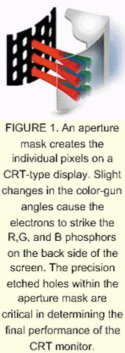
Television sets, computer monitors, and nearly all other displays based on CRTs rely on an aperture mask to control the intensity and color of the screen pixels. Concealed behind the phosphor coatings on the inside of the glass face plate, these complex masks, sometimes called shadow masks, are produced from steel or nickel-alloy sheets with a typical thickness of 0.007 in. (0.18 mm). Small holes or slots are formed by precisely etching the material to form what resembles a finely meshed screen (see Fig. 1). The size, form, position, quality, and orientation of these etched holes are critical in determining the final performance of the finished display.
The size and geometry of the precision etched holes depend mainly on the type of CRT display being manufactured and also on subtle differences and variations related to the manufacturer and the material type. Geometry changes can also occur within a given mask depending on the location of holes. Holes in the center of the mask tend to be symmetrical, whereas holes near the edge of the screen tend to be asymmetrical due to increasing angles subtended from the center position of the electron guns. In the case of television masks, the etched holes resemble rectangular slots with typical dimensions on the order of 150 x 450 µm.
Close examination of a television (non-HDTV) reveals that the individual pixels are actually a series of small dashes (see Fig. 2). The high-magnification image discloses that these precision etched holes are elongated with well-defined sidewalls (called cones) that are not perpendicular to the surface. This image, taken near the top edge of a television monitor, also shows the asymmetry present between the front side of the hole (larger rectangular dimensions) and the through-part of the hole (small slots). The slots are not centered within the larger rectangular dimensions. For proper operation of the picture tube, the quality and orientation of these precision etched holes are critical.
In comparison, high-resolution monitors, such as those found in computers, use a series of finely pitched circular or elliptical holes in a honeycomb pattern (see Fig. 3). Typical hole sizes are on the order of 100 µm, with center-to-center distances of 280 µm, which is the standard 0.28-mm commercial monitor-resolution specification. Here, the cones resemble small countersunk holes, similar to those of television masks. The concentricity of the upper and lower edges varies as a function of their position on the mask, especially as monitor sizes continue to increase.
Independent of mask type, both configurations rely on complex photo-etching processes that strive to control the ultimate hole size, location, and other parameters that ensure a precision etched cone rather than a straight-sided hole. Even though the manufacturing of these devices has been defined for decades, the yields and quality-control methods have been significantly below other industry thresholds.
Other defects that render poor performance in the finished CRT display include incorrect hole size, missing holes, improper cone angles, and a phenomenon called etched surface area. Because a single improperly etched hole results in a bad pixel, easily seen in the finished CRT, it is imperative that the aperture masks be 100% inspected. In many cases, more than 1 million precision holes are used within a single mask, making 100% inspection highly complex.
Quality and yield
From a quality-control standpoint, it is critical to remove all defective masks from the end of the manufacturing stream before shipment to the tube manufacturer. For example, an aperture mask worth an average of $5 is eventually encased within a finished CRT that may be worth almost $200. The CRT manufacturing process is irreversible, and the final quality of the aperture mask cannot be fully determined until the CRT is operated. Consequently, a defective mask renders the entire CRT with either sub-par quality or, in many cases, useless.
FIGURE 5. These monitor masks demonstrate the two distinct binary solutions available for the solution to this application. While these images are identical with respect to any subsequent digital-signal processing hardware or software, they represent entirely different patent-pending lighting schemes.
These quality issues have measurable costs associated with them that can multiply the actual associated part costs. Automated inspection techniques, therefore, have the potential to deliver higher product quality, while at the same time lowering labor costs. The combination of simultaneously improving both customer satisfaction and bottom-line profitability is currently driving the pursuit for automated solutions to these inspection challenges.
Additional financial incentives exist on the yield side of the equation. Current production facilities throughout the world operate with yields that range between 60% and 80% and that may dip as low as 45% for extended periods of time. With the comparatively high cost of a production hour within these facilities, and the associated cost of producing scrap material, manufacturers stand to gain production-cost benefits if new automated inspection technologies can eventually provide real-time process-control information. This information can then be fed back upstream so that production-process changes can be implemented rapidly.
While there are more than 30 different industry-standard defect types, the majority of critical defects that occur regularly can be summarized as defects for which the etching boundaries have not been properly controlled. Either the through-hole is under- or over- etched, the cone walls are under- or over-etched, or the land area has been improperly etched. There are many potential process reasons that any one of these conditions might exist, but from a strictly quality control standpoint, these are the basic and logical breakdowns for the process related defects that occur in a normal production environment.
Inspection techniques
The sheer number of holes within a typical aperture mask, combined with their minute size, challenge any inspection process. In the past, human inspectors have been trained to spot a variety of gross level defects with marginal success. In performing eye evaluations, human inspectors bend and flex thin screens in front of light tables to detect singular pixel defects in masks that now regularly have in excess of 1 million precision holes. Typical of the comparison between human inspectors and machine-vision solutions, the a perture-mask-inspection task is much more suited for the tireless and quantitative excellence that only automated inspection techniques can provide.
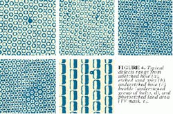
Over the years, a variety of laser and white-light techniques have been developed and adopted to provide some form of densitometry measurement with varying levels of success. While these techniques have been helpful in eliminating many of the gross defects prior to end-of-the-line inspection stations, in general, they lack the specificity to detect and classify these defects (see Fig. 4).
The problem with most current off-the-shelf (COTS) machine-vision systems is that they are not adequately equipped to handle patterned inspection tasks. Relatively small defect areas within many regularly spaced features provide sufficient computational overload to render general-purpose vision machines and COTS software and hardware useless. For example, obtaining the required resolution under normal production conditions mandates the use of a 4-k linescan camera running at 8 kHz. Moreover, if 8 bits are also needed, then the system must process 262 kbytes of patterned gray-scale information per second. Processing an average 36-in.-wide web requires 18 such cameras, making the total processing load approach 5 Mbytes/s, well outside the range of existing COTS systems.
The key problems are raw data speed and sufficient processing algorithms. Typical golden-template-based algorithms require expensive high-speed subtraction routines and incur major problems when used with acceptable real-world process variations. If subsequent scaling is required in an attempt to reduce the associated system noise, the processing time and related costs put this approach out of reach.
Optical preprocessing
The speed at which optical information is transformed under typical and routine interactions is unrivaled. An inspection approach based on this technology centers around the fact that optical processing of information takes place at times that are, for all practical purposes, instantaneous and at costs that are much less than computing hardware or software solutions. One such method, called optical preprocessing, describes a host of potential solutions that take advantage of the power of light before applying additional hardware or software solutions.
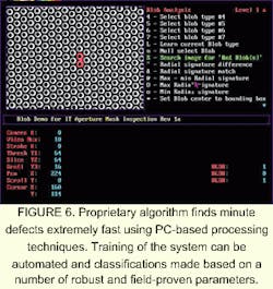
In the case of inspecting aperture masks, previous attempts tried unsuccessfully to apply standardized gray-scale imaging techniques. These inspection problems can be eliminated by optical preprocessing to a completely binary system (see Fig. 5). The major problems associated with this application, and many similar patterned applications, focus on data compression (see Fig. 6).
MIKE MUEHLEMANN is president of Illumination Technologies Inc., East Syracuse, NY 13057; e-mail: [email protected].


