Ultraviolet light checks circuit-board flaws
To detect component placements on circuit boards, a vision inspection system 0looks for embedded ultraviolet-sensitive blue dots.
By Lawrence J. Curran,Contributing Editor
A novel vision-system technology that uses ultraviolet (UV) light to inspect printed-circuit boards (PCBs) for missing and skewed surface-mount devices promises to boost board-inspection yields. The system detects shorts between the leads of fine-pitch integrated circuits (ICs), as well as other defects. Mike Feld, president of Original Solutions Inc. (Saint Laurent, QC, Canada), guarantees users a board-yield increase of as much as 50%.
Original Solutions developed the patented concept, which has been implemented in a system integrated by InoSys Inc. (Naperville, IL). Called the DOTector Vision Inspection System, it targets customers who need to increase both throughput and yields for PCBs with surface-mount components.
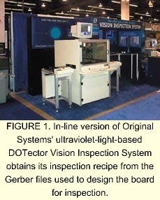
FIGURE 1. In-line version of Original Systems' ultraviolet-light-based DOTector Vision Inspection System obtains its inspection recipe from the Gerber files used to design the board for inspection.
InoSys and Original Solutions initially began the system integration with a prototype, which is an off-line version. They also developed an in-line production-oriented vision inspection system that can inspect as many as 300,000 components per hour (see Fig. 1). The system differs from other approaches in that it uses UV light to detect assembly flaws, omissions, misplacements, misalignments, shorts, and polarity checkpoints on all leaded packages down to a 10-mil pitch.
"We had the idea to turn around the way automated optical inspection systems look at PCBs, but we needed someone to put hardware and software around it," Feld says. "We came up with what is essentially a PCB with UV-sensitive markings. The vision system sees this signature as light, while everything else is black," he explains.
Feld says InoSys president Rich Schwarzbach has frequently evolved novel platforms for vision problems. InoSys convinced Feld that the company could identify the signature markings with a minimum of false detections, "which is a problem for many automated-optical-inspection systems."
In the Original Systems' concept, the supplied Gerber computer-aided-design (CAD) file is modified by the end user whose boards are to be inspected. A Gerber file is an industry-standard format for using Gerber photo plotter files. These are CAD programs that generate photoplots for manufacturing printed-circuit boards, including the metal routing and component pad placement. The photo plotter technology was developed by Gerber Systems, which was later purchased by Barco ETS (Gent, Belgium).
FIGURE 2. The large white area in the image with the red border is the "blue dot" beneath a component. The visible dot means the part is missing. The red border indicates a failure. The green outlines show the locations of other blue dots, but a component is covering them, indicating that the parts are properly placed. The green lines are superimposed over the blue dots located between the leads of IC packages. Because the dots are visible, those locations are clear of solder or material; there is no short and the indicator is green.
The inspection points are built in at the same time that the boards are designed, and the boards are built by the board fabricator. Feld did not reveal all the details of the patented process, saying only that the board fabricator uses the Gerber file to "add our technology to the board."
The inspection points are embedded by photoimaging blue dots, which are sensitive to UV light, in appropriate locations on the PCB (see Fig. 2). Feld says that no halides or acids are used, "and there's no residue of any kind." Nor does signature embedding require any extra steps or add more costs to the board-fabrication process, he claims.
Integration challenges
InoSys' Schwarzbach says that because of the abundance of unknowns in the manufacture of surface-mount PCBs—especially the plethora of chip manufacturers, chip-form factors, and variations of chip cosmetics—the vision inspection system had to be designed to minimize interference and confusion among component types. It also had to maximize the features of interest without requiring special programming and constant user intervention.
One key system element is an M300 camera from JAI AS (Glostrup, Denmark) that uses a 2/3-in. CCD imager with adjustable gain controls. The camera was selected for its versatility and large imager size, which maximizes its sensitivity to low-light levels.
FIGURE 3. Board builders need a Gerber file to design and fabricate a printed-circuit board (PCB). The Gerber file allows the embedding of all the calibration tools needed to incorporate system vision into the file, which yields a calibration master within each board being inspected.
Schwarzbach says another key requirement was a light source that is rich in the UV spectrum, safe because it presents a unified field of vision, and allows the least amount of light to pass through. "We needed a lens and lighting system that highlights the object of interest while de-emphasizing the background," he points out.
To reduce the effects of lens aberrations, InoSys chose a Computar TEC 55—a telecentric 55-mm lens—from CBC (America) Corp. (New York, NY). The lens overcomes the usual CCTV lens perspective aberrations by providing a depth of field that allows off-center objects to be the same size as those at the center. The other half of the lens and lighting tandem is a dual-circular ring light from StockerYale Inc. (Salem, NH). It uses black fluorescent bulbs to provide "the most uniform UV-rich lighting we could find," Schwarzbach says.
"Because of the research nature of the project initially, we chose a software package that gave us considerable flexibility in pre- and postprocessing of the [Original Solutions] algorithms," Schwarzbach says. InoSys chose Sherlock software from Coreco Inc. (St. Laurent, QC, Canada). Furthermore, because the inspection system had to interface with other machines in a shop-floor network, InoSys chose an open system architecture that uses a standard personal computer (PC), a PC-based frame-grabber board, and software.
The prototype inspection system uses a Coreco PC Vision frame grabber, which Schwarzbach describes as "a robust, multicamera frame grabber with excellent camera and triggering controls. This frame grabber interfaces easily with the features of the M300 camera and the Sherlock software." Production units use Coreco MV-tools from which the Sherlock program is derived.
The PC is built around a 900-MHz AMD Thunderbird microprocessor from AMD Inc. (Sunnyvale, CA). It includes 128 Mbytes of RAM and runs the Microsoft Windows 2000 operating system.
Gerber connection
Schwarzbach says that after InoSys engineers understood the Original Solutions' embedded-signature concept, "we wanted to build an automated system that could inspect various anomalies—including missing or extra surface-mount devices, misalignment, tombstoning, shorts, and so forth, and we wanted to do it without the user being required to do any programming." The first assumption InoSys made is that all board builders need a Gerber file to design and fabricate a PCB. Schwarzbach explains, "Our system could learn anything it needed to be taught from the Gerber file. We concluded that if a PCB maker can build a board [using a Gerber file], we can inspect the board."
Additionally, using the Gerber file "allowed us to embed all the calibration tools necessary for machine vision into the file, yielding a 'calibration master' within each board being inspected. The machine therefore can recalibrate itself for changes in scale, rotation, or board configuration automatically, without user intervention," he adds.
A key challenge for InoSys was to develop an x-y stage that could be controlled by the vision inspection system to accurately position a PCB as large as 18 x 24 in. opposite the camera. In the prototype system, the company determined that moving the board under the camera would lessen the number of variables affecting the vision inspection.
If the camera is perpendicular to the PCB but the stage isn't perfectly leveled, "the system doesn't see much of the angle change when the board moves under the camera," Schwarzbach points out. But if the board remains still and the camera is moved, the aberrations are pronounced. Therefore, InoSys decided, for the prototype design, to suspend the camera over the board to be inspected, and move the camera in both the x- and y-axes. In the production inline vision inspection system, the camera moves in the x-axis while the board moves in the y-axis.
The in-line machine is equipped with industry-standard Surface Mount Equipment Manufacturer Association (Northbrook, IL) controls that plug directly into existing upstream and downstream production machines. When the upstream machine has a PCB available for inspection, it signals the inspection system to accept the board. The user chooses, from a standard Windows drop-down menu, the name of the board being inspected. Then the system reads the proper modified Gerber file to obtain its inspection criteria (see Fig. 3 p. 26).
FIGURE 4. Light spaces (blue dots) visible beneath several components?located along the bottom and right edges and at the top right?indicate improper placement or missing components. The dark lines across several leads at bottom and right also indicate short circuits. This board would be sent to a repair station.
The movable y-axis conveyor of the inspection system gathers the waiting board, moves it to the inspection location, clamps it to eliminate slip, and begins the calibration and inspection processes. Data are automatically logged to a database, and, depending on user needs, the system halts on a defect or simply logs the data. Upon completion of the inspection process, the system's conveyor moves the board to an offload position—either to a continuation conveyor for further processing or to a repair loop or queue.
The prototype is an off-line system, not intended for production-line use. This system has all of the features of the in-line machine, except that an operator must load and unload each panel of PCBs. It is appropriate for use in incoming inspection, quality control, or other audit areas of a factory. Schwarzbach says InoSys has a strategic alliance with PCT Automation Systems (Addison, IL), which makes transfer conveyors for PCBs that pick up, pass along, and position a board for inspection.
Original Solutions will add other devices so that the vision inspection system interfaces easily and properly with other equipment, such as a repair station or a repair queue. For example, a graphical user interface can be used by a repair cell after a board is inspected to extract information from a structured-query-language database to make repairs (see Fig. 4 p. 32). In that scenario, using the in-line system, a PCB would move by conveyor to the vision inspection system, which has been "automatically" programmed using the Gerber file that controlled surface-mount device insertion.
"The inspection system takes the Gerber data, starts inspecting, and delivers it to a repair cell or on to the next step," Feld says, which may be reflow soldering, final inspection, or testing. He says that the rate of inspection is as high as 300,000 components per hour using one camera, and that the system logs no false detections for the defects that are programmed.
Attitude adjustment
Feld says that by using a customer's specific board data to modify the Gerber file in embedding the UV signature, the system changes the way boards are inspected. It eliminates the concept of "golden boards" and the need for programming that's required to teach an inspection system those conditions that depart from the norm. Schwarzbach says that the value InoSys adds is that the vision system is looking for exactly what it is designed to look for. It's a complete closed-loop system, with real-time feedback from the board. It's simply looking for the embedded blue dots.
"We've created an open-system architecture," Feld says. "and users can retrofit it to systems already in place."
__________________________________
COMPANY INFORMATIONAMD Inc.Sunnyvale, CA 94088Web: www.amd.comCBC (America) Corp.
New York, NY 10150-5330
Web: www.cbcamerica.com
Coreco Inc.
Saint Laurent, Quebec, Canada H4T 1V8
Web: www.imaging.com
InoSys Inc.
Naperville, IL 60185
Web: www.inosys.com
JAI AS
DK-2600 Glostrup, Denmark
Web: www.jai.com
Original Solutions Inc.
St. Laurent, Quebec, Canada
H4T 1T3
Web: www.original-solutions.com
PCT Automation Systems
Addison, IL 60101
Web: www.pcti.com
StockerYale Inc.
Salem, NH 03079
Web: www.stockeryale.com

