Time of Flight sensors target high-speed 3D machine vision tasks
While many companies developing 3D machine vision products use off-the-shelf image sensors for image capture, several manufacturers now offer image sensors specifically designed for 3D vision. Having become increasingly available in recent years, Time of Flight (ToF) represents one such example.
ToF technology works by illuminating a scene with a modulated light source and observing the reflected light. The phase shift between the illumination and reflection can be measured and translated to distance. In some devices, a pulse-based measurement technique is implemented.
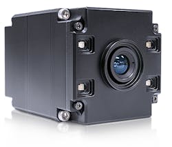
Several companies now offer ToF sensors, including those as small as 32 pixels and up to 1.3 MPixels. Part of the DepthSense ToF sensor series from Sony (Tokyo, Japan; www.sony.com), the IMX556PLR back-illuminated image sensor delivers 640 x 480 resolution at a 6 m working distance at 30 fps. LUCID Vision Labs (Richmond, BC, Canada; www.thinklucid.com) incorporates the sensor into its Helios Time of Flight camera (Figure 1).
"Sony has a history of leapfrogging current sensor technologies and the DepthSense IMX556PLR Time-of-Flight sensor was no different, as it greatly improved 3D accuracy and precision over existing ToF sensors,” says Rod Barman, Founder and President at LUCID Vision Labs. “LUCID leveraged this improved 3D performance in a compact camera design to get the Helios ToF camera fast-to-market [July 2019] and subsequently deployed in applications across several industries.”
To maximize performance for the IMX556PLT sensor, LUCID developed a proprietary depth processing pipeline to produce accurate and precise depth data. The processing pipeline is implemented on the FPGA inside the Helios camera and on the NVIDIA GPU for the new Helios Flex ToF module, which connects to an embedded system using the NVIDIA Jetson TX2. Featuring Sony’s depth sensing technology, this module allows developers to leverage a high-performance, ToF camera on a cost-effective, compact embedded system, says Barman.
Related: Understanding the latest in high-speed 3D imaging: Part one
Basler (Ahrensburg, Germany; www.baslerweb.com) also deploys the IMX556PLR in its forthcoming blaze ToF camera, while Seeed Technology Co., Ltd. (Shenzhen, China; www.seeedstudio.com) bases its DepthEye Turbo ToF camera around it as well.
In addition to the Sony sensor, Basler integrates ToF sensors from Panasonic (Osaka, Japan; www.panasonic.com) into one of its 3D cameras. The sensor is a 640 x 480 ToF sensor offering a frame rate of 20 fps and a working range of up to 13 m. In addition to this sensor, Panasonic also developed a long-range ToF sensor based on 250,000 avalanche photodiode pixels capable of capturing 3D range imaging at up to 250 m, even at night, according to Panasonic.
Additionally, with some computational imaging techniques involved, Sony’s Polarsens line of polarization image sensors can acquire cursory 3D images. To accomplish this, the four polarization angles of light hitting the sensor are decoded, creating a photometric 3D view of an object, says David Dechow, Principal Vision Systems Architect, Integro Technologies (Salisbury, NC, USA; www.integro-tech.com).
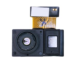
ifm efector, inc. (Essen, Germany; www.ifm.com) subsidiary pmdtechnologies (Siegen, Germany; www.pmdtec.com) developed a CMOS 3D ToF sensor based on its own pmd pixel matrix in collaboration with Infineon Technologies (Neubiberg, Germany; www.infineon.com). Sold by Infineon, REAL3 ToF sensors feature resolutions from one 3D pixel up to 640 x 480 3D pixels (Figure 2).
In addition, pmdtechnologies sells PC-based development kits like the pico flexx module, which features a 224 x 172 sensor, frame rates up to 45 fps, and a measurement range of 0.1 to 4 m, while the pico monstar module features a 352 x 288 sensor, frame rates up to 60 fps, and a measurement range of 0.5 to 6 m. The company also now offers development kits for embedded systems.
For consumer electronics and mobile designs, pmd/Infineon-based depth modules are available from a number of companies, including LG Innotek (Seoul, South Korea; www.lginnotek.com/en) which provided the ToF module for the 3D face identification in the LG G8 mobile phone launched in early 2019. More mobile phone designs with pmd/Infineon depth modules were released in 2020, with more on the way.
Related: Understanding the latest in high-speed 3D imaging: Part two
“Due to the popularity of the design in mobile phones, pmd and Infineon are increasing the capacity and throughput of the technology which is lowering the price for all users,” says Mitchell Reifel, VP Business Development and Sales, at pmdtechnologies.
ESPROS Photonics (Sargans, Switzerland; www.espros.com) manufacturers three ToF System on Chips (SoC), which it deploys into its line of ToF modules. A fully integrated 3D ToF imager, the flagship epc660 chip has a resolution of 320 x 240 pixels. Apart from the actual CCD pixel field, the chip includes complete control logic to operate the device. Additionally, the chip offers a speed of 65 full frame TOF images per second and 12-bit parallel video interface.
Offering a similar design but with a 160 x 60-pixel array, the epc63 chip offers a speed of up to 128 fps in full 3D ToF mode. Meanwhile, the company’s epc611 chip is a general purpose, fully integrated CMOS device for optical distance measurements and object detection that features an 8 x 8 CCD array. All ToF chips also offer over 70% quantum efficiency at 905nm, ambient light suppression at up to 130K lux, and transfer speeds up to 250MHz.
Offering a similar design but with a 160 x 60-pixel array, the epc63 chip offers a speed of up to 128 fps in full 3D ToF mode. Meanwhile, the company’s epc611 chip is a general purpose, fully integrated CMOS device for optical distance measurements and object detection that features an 8 x 8 CCD array.
In its OPT8241 ToF sensor, Texas Instruments (Dallas, TX, USA; www.ti.com) combines ToF sensing with an analog-to-digital converter and a programmable timing generator that controls reset, modulation, readout, and digitization sequence. The CMOS device offers 320 x 240 resolution at frame rates of up to 150 fps and through its built-in timing generator, can optimize for such depth sensing performance metrics as power, motion robustness, signal-to-noise ratio, and ambient cancellation.
Designed with an integrated infrared laser light source and internal clock sources, the AFBR-S50MV85I from Broadcom (San Jose, CA, USA; www.broadcom.com) is a 32 pixel ToF sensor that targets optical distance and motion measurement. Broadcom bases its sensors on a correlation (phase shift) ToF measurement principle. The company developed the sensor with a focus on applications requiring high speeds (up to 3,000 fps) and accuracy at medium distance ranges, with small size and low power consumption (5V). All AFBR-S50 sensors, according to the company, show exceptional performance in daylight, have a high accuracy <1% (total range), and have no interference with other sensors. The AFBR-S50 sensor platform includes several sensor variants which differ in light source (850 nm, 680 nm, w/o lighting), maximum ranges from 3m to 30m, as well as resolution and field of view.
Broadcom also makes the AFBR-S50MV85G, which is based on the same ToF sensor and has an integrated 850 nm VCSEL laser light source and uses a single voltage supply of 5V.
Additionally, the AFBR-S50MV85G-EK evaluation kit comes with a Laser Class 1 eye safe laser, ARM Cortex M0+ board, adapter board with soldered sensor, and a USB cable and supports up to 400 fps with up to 16 illuminated pixels
Melexis (Ieper, Belgium; www.melexis.com) manufactures several ToF sensors and chipsets, including the 640 x 480 MLX75027 automotive ToF sensor. This model captures up to 135 fps, supports both the 850 and 940 nm wavelength, and has integrated light source control with up to 100 MHz modulation frequency. Another automotive ToF sensor made by the company, the MLX75024, has 320 x 240 pixels, supports both the 850 and 940 nm wavelength. MLX75024 works together with MLX75123 ToF companion chip, which provides all the control signals and light source control with up to 40 MHz modulation frequency. Both sensors feature Sony’s DepthSense ToF technology in its pixels.
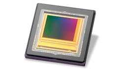
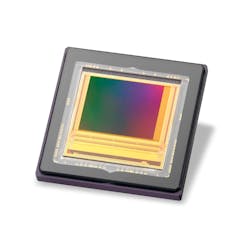
Offering higher-resolution, Teledyne e2v (Grenoble, France; www.teledyne-e2v.com) makes a 1.3 MPixel CMOS image sensor with its Bora ToF sensor (Figure 3). The sensor has a 10 µm pixel size, 1280 x 1024 resolution, and a gating time of 42 ns. Features listed by the company include scene capture with large field of view in both 2D and 3D, real-time 3D image capture at over 30 fps, and short- and long-range capabilities that according to the manufacturer are robust to ambient light intrusions via a unique HDR feature.
Teledyne e2v also offers an evaluation kit for the sensor, which includes a compact, 1-in. optical format calibrated module, a light source for near infrared illumination, and optics targeted at ToF capture for short-range distances up to 5 m, or mid-range distances up to 10 m.
Related: 3D machine vision guides robotic system for logistics e-fulfillment
“Our newest Time-of-Flight sensor offers a high spatial resolution of 1.3MPixels, which provides larger field-of-view coverage,” says Ha Lan Do Thu, Marketing Manager, 3D Business Team. “This is important for our customers that are seeking to optimize their systems and save costs. In addition, the sensor achieves excellent precision and accuracy in 3D measurements at a true 1.3MPixel depth resolution and can handle both short and long-range capture (over 10 meters) in outdoor conditions.”
Additionally, in its latest Kinect camera, the Azure Kinect, Microsoft (Redmond, WA, USA; www.microsoft.com) deploys a proprietary 1 MPixel ToF sensor. The sensor features a 3.5 mm pixel size, 512 x 512 analog binning, and provides 640 x 576 or 512 x 512 at 30 fps, or 1024 x 1024 at 15 fps.
Trends and technologies evolve quickly in machine vision. New image sensing technologies could soon emerge that redefine 3D imaging cameras and applications. For that reason, the next issue of Vision Systems Design will cover novel image sensor designs that power 3D imaging cameras and applications.
Companies mentioned:
Basler
Ahrensburg, Germany
www.baslerweb.com
Broadcom
San Jose, CA, USA
www.broadcom.com
ESPROS Photonics
Sargans, Switzerland
www.espros.com
ifm efector, inc.
Essen, Germany
www.ifm.com
Infineon Technologies
Neubiberg, Germany
www.infineon.com
Integro Technologies
Salisbury, NC, USA
www.integro-tech.com
LG Innotek
Seoul, South Korea
www.lginnotek.com/en
LUCID Vision Labs
Richmond, BC, Canada
www.thinklucid.com
Melexis
Ieper, Belgium
www.melexis.com
Microsoft
Redmond, WA, USA
www.microsoft.com
Panasonic
Osaka, Japan
www.panasonic.com
pmdtechnologies
Siegen, Germany
www.pmdtec.com
Seeed Technology Co., Ltd.
Shenzhen, China
www.seeedstudio.com
Sony
Tokyo, Japan
www.sony.com
Teledyne e2v
Grenoble, France
www.teledyne-e2v.com
Texas Instruments
Dallas, TX, USA
www.ti.com
About the Author

James Carroll
Former VSD Editor James Carroll joined the team 2013. Carroll covered machine vision and imaging from numerous angles, including application stories, industry news, market updates, and new products. In addition to writing and editing articles, Carroll managed the Innovators Awards program and webcasts.


