Sensor and camera requirements for hyperspectral imaging
Lu Cheng, Brad Coyle, and Albert Tu
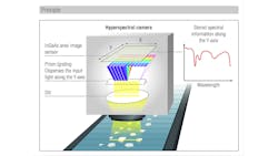
Initially used for Earth observation, hyperspectral imaging (HSI) technology has expanded into various fields, from industrial sorting to medical research where, for example, scientists use the technique to generate databases for skin and subcutaneous tissues. Hyperspectral imaging combines the benefits of a camera and a spectrometer (Figure 1), and simultaneously collects both spatial and spectral information.
With the improvement of image sensors and cameras, researchers and developers are finding more and more applications for hyperspectral imaging today, including food quality control, pharmaceutical process control, plastic sorting, and biological measurements.
Example applications
Food quality control
In the past, food quality control required destructive measurement. Quality assurance personnel chose one sample in each lot for sampling, inspected its appearance, and used destructive measurement techniques to define the grade based on the analysis results. Now, SWIR hyperspectral imaging can help identify and quantify the chemical components of a food product, providing information such as nutrition, fat percentage, sugar level, and freshness based on the distinct wavelengths, or spectral fingerprint, of each molecule analyzed. For example, a SWIR hyperspectral camera on a drone can help measure the sugar content in apples growing on a tree, and to forecast the grade and quality before harvest season.
Plastic sorting
In 2017, the US had an 8.4% recycling rate for plastic (bit.ly/VSD-EPA), yet recycling plants receive 3 million tons of plastic per year (Figure 2a). With the growth of recycling awareness, more people are expected to recycle their waste, which means more plastic for recycling plants to process. However, different plastic materials require different recycling processes, and the inability to differentiate them could leach toxic chemicals if the wrong process is used, or damage the instrument during the process. With hyperspectral imaging, recycling plants can easily differentiate plastic materials using 1.7 to 2.6 µm spectral information and mark the position on the conveyor belt using the spatial information collected from the camera (Figure 2b).
Types of hyperspectral imaging
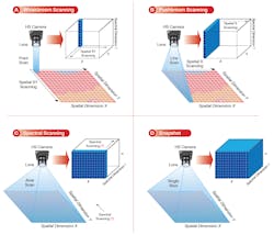
Hyperspectral cameras can capture information in four ways: whiskbroom (point scanning) cameras, pushbroom (line scanning) cameras, cameras based on spectral scanning (area scanning or plane scanning), and snapshot (single shot) cameras.
Whiskbroom cameras capture one single pixel at a time (Figure 3a). The image builds as the camera raster scans across the sample, and contains all its spectral information. While very time-consuming during the image acquisition, the method results in a very high spectral resolution.
Related: Hyperspectral imaging system grades agricultural products
Faster than whiskbroom cameras and offering high spectral resolution, pushbroom cameras capture one line at one time (Figure 3b). The camera scans this line across the sample to generate the full image. Although faster than whiskbroom, pushbroom cameras may produce aliasing and movement artifacts in resulting images.
Spectral scanning cameras gather the entire spatial information for a given wavelength at one time (Figure 3c). A hyperspectral cube generates based on one image/one wavelength at a time. While fast per image, spectral scanning produces cubes slowly due to the time required to change wavelengths.
Hyperspectral snapshot cameras can capture hyperspectral video (Figure 3d) and are fast and ideal for imaging moving objects. These cameras typically offer limited spectral and spatial resolutions, however.
Image sensor requirements
Independent of the hyperspectral platform, the optical sensor plays the most important role in data acquisition. In this section, the article covers the sensor specifications required for HSI.
Spectral response range
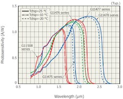
Compared to the traditional RGB imaging, HSI’s major advantage lies in its ability to capture more details over a wider spectral response range with a higher-resolution spectrum. With silicon technology like CCD and CMOS image sensors, discoloration and some foreign objects in a meat product, for example, can be detected in the visible and near-infrared range, from 400 nm up to 1100 nm wavelengths. However, detecting the water content of meat (tenderness) using the reflectance imaging method requires a spectral range of 900 to 1700 nm. In this wavelength range, the CCD and CMOS sensors do not have sufficient response, while the standard InGaAs technology can achieve more than 70% quantum efficiency at a decent cost.
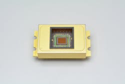
As another example, detecting the fatty acids in beef requires the 1000 to 2300 nm spectral range. With the extended InGaAs technology, the sensor can detect from 900 nm up to 2.5 µm wavelengths, making it suitable for hyperspectral imaging beyond 1.7 µm. As one of a few suppliers that can offer an InGaAs area image sensor with the extended wavelength, Hamamatsu Photonics (Hamamatsu City, Japan; www.hamamatsu.com) released a series of QVGA InGaAs area image sensors with the cutoff wavelength of 1.7 µm, 1.9 µm, 2.2 µm, and 2.5 µm (Figure 4).
Dynamic range
The optical sensor’s dynamic range is very important to acquiring information in a wide spectral range, especially when deploying pushbroom technology for image acquisition. Pushbroom cameras capture a whole image line simultaneously with spectral information and exposure time can be set at only one value for all wavelengths, so the sensor needs to have sufficient dynamic range to acquire very low-level signals and the peak signals across the whole spectrum. The dynamic range depends on both the readout noise and the saturation level of a sensor. The readout noise typically determines the minimum signal level that a sensor can detect. For example, 800 µV rms readout noise is required to achieve 1500 dynamic range at 1.2 V saturation output level, which is not easy for the CMOS ROIC design. At a long exposure time, the dark current shot noise requires consideration, especially when using the extended InGaAs. For example, with the same pixel format, if a standard InGaAs sensor (1.7 µm cutoff wavelength) has its dark current specified as 0.03 pA, then an extended InGaAs sensor (2.5 µm cutoff wavelength) can have its dark current specified as high as 30 pA.
Related: Novel broadband LED enhances hyperspectral imaging applications
Sensitivity
Compared to traditional spectroscopy where the exposure time can be set as long as ~30 seconds, the exposure time for HSI must be short enough (sometimes in the milliseconds, even microseconds, range) to avoid saturation at any wavelength, which could result in underexposure of some spectral bands and low accuracy of the spectral measurement if the sensor does not have sufficient sensitivity at any wavelength. A sensor’s sensitivity includes the photodiode array’s photosensitivity and the on-chip readout circuit’s charge-to-voltage conversion gain. The readout noise level typically increases with the increasing sensitivity, however. With the area-scanning HSI technique, a suitable exposure time or on-chip gain can be set for each wavelength. For example, a long exposure time or high conversion gain can be set for the low-signal range, while a short exposure time or low conversion gain can be set for the strong-signal range in order to obtain smooth output spectra in the entire wavelength range. Hamamatsu Photonics offers both linear and area InGaAs image sensors with programmable, on-chip charge-to-voltage conversion gain.
Rapid acquisition: IWR and ROI
As the most popular hyperspectral imaging approach, the pushbroom method stores the hyperspectral data cube in the format of band-interleaved-by-line (BIL)—a scheme of continuous scanning in one direction. For this reason, pushbroom cameras particularly suit conveyor belt systems commonly used in industrial processes such as food quality and safety inspection, sorting in recycling plants, and pharmaceutical labelling and packaging. For applications with fast moving objects, rapid acquisition becomes critical. Not only the short exposure time but also the architecture of the sensor design can improve the readout speed. For example, the on-chip sample-and-hold circuit enables the integrate-while-readout (IWR) feature, so the sensor can start the second exposure while the whole line (with data from the previous exposure) reads out.
The area-scanning method records both spatial and spectral information in a series of wavelengths, making it attractive for fast imaging applications, but area scan cameras do not suit applications requiring moving sample measurements. Hamamatsu Photonics makes area image sensors with the column parallel structure and the partial readout (ROI) feature, which not only can shorten the readout time proportionally to the number of pixels, but also save data storage and data processing efforts.
Camera requirements
Cameras
Hyperspectral imaging cameras come in two types: line scan and area scan cameras.
Line scan cameras integrate a linear, 1D sensor and offer the advantage of high frame rates, at more than 40,000 lines/s, making it suitable for inline inspection on assembly lines. When combined with artificial intelligence (AI) for defect identification or pattern recognition, it is a valuable part of an inspection system, as high acquisition speeds enable AI-based sorting and defect identification tasks.
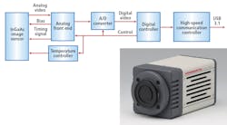
Area scan cameras integrate a 2D sensor and offer high spatial information by generating snapshot images of a whole scene. Typical area scan InGaAs cameras come in QVGA or VGA formats (Figure 5a). The cameras can capture many images quickly, provide a large field of view, and suit wide area imaging applications in agriculture.
Hyperspectral imaging cameras also deploy into food inspection, security, plastic sorting, and drug discovery. Most cameras have cooling on the sensor that lower the noise and dark current, improving overall image quality. On-board memory or user-accessible FPGA makes cameras very attractive for customization.
Interfaces
Interface choice represents an important consideration for choosing a camera, as it defines the camera speed, connectivity, and how well it integrates with the rest of an instrument (Figure 5b). Cameras come in many interfaces designed for different purposes. USB and GigE are the most commonly encountered, while examples include RS-422/LVDS, Camera Link, RS-232, and CoaXPress interfaces.
Software support
Pairing the right software with hyperspectral hardware represents a crucial step in system development. Hardware driver support must be considered, as the camera must function in a chosen software environment. Many third-party software platforms, such as LabVIEW from National Instruments (Austin, TX, USA; www.ni.com) and MATLAB from MathWorks (Natick, MA, USA; www.mathworks.com), VisionPro from Cognex (Natick, MA, USA; www.cognex.com), and IMPACT from Datalogic (Bologna, Italy; www.datalogic.com), exist today that integrate well with different camera manufacturers.
Software development kit support represents a major consideration for users looking to self-program an interface. Writing a custom interface allows users to have full control over the end-user’s experience. Python and C++ are common programming languages, while the Linux operating system provides great flexibility for controlling devices and data flow. As a developer, one must confirm that a camera supports these programming tools or enter a costly system redesign.
Conclusion
Hyperspectral imaging combines the features of a camera and a spectrometer. Collecting spectral and spatial information at the same time saves both time and money by using one camera instead of both a spectrometer and a camera. Past image sensors and cameras have had limitations in speed, resolution, sensitivity, and software. New advances in technology have made hyperspectral imaging easier than ever. Companies such as Hamamatsu Photonics have developed image sensors and cameras that offer high speed, high resolution, and high sensitivity. Improved software and programming tools make it easy to integrate hyperspectral imaging for any application. There are many options available for hyperspectral imaging today.
Lu Cheng is Senior Applications Engineer, Brad Coyle is OEM Camera Product Manager, and Albert Tu is Marketing Engineer at Hamamatsu Photonics (Hamamatsu City, Japan; www.hamamatsu.com)
