High-speed cameras and Camera Link
Although alternate interfaces offer some advantages, Camera Link will remain the interface of choice for high-speed applications.
By Joseph Sgro and Paul Stanton
Currently, Camera (Channel) Link is the preferred moderate-to-high-speed camera interface. Behind this dominance, however, is the fact that the high-performance camera market had consisted almost entirely of proprietary CCD devices, which were not only expensive but also offered low data or frame rates because of manufacturing costs. CMOS image sensors had low image quality and thus were unsuitable for the imaging and machine-vision markets.
This situation has changed in the last several years, and companies such as Cypress (formerly FillFactory), Dalsa, and Micron Technology have begun selling new models of CMOS sensors that offer high image quality and a high frame rate at relatively low cost. Impressed by their performance, FastVision began using some of these new sensors in its FastCamera series.
The CMOS sensors used in the FastCamera series have data-output rates that can exceed 1 Gbyte/s. Such rates significantly surpass most current computer-processing and external interconnect standards, except Camera Link. Thus, productive use of these high-speed sensors presents a severe challenge to engineers. Nonetheless, trends toward increased processing and transfer rates inevitably will push the processing and interconnect paradigms currently used in camera designs to levels requiring use of either complex Camera Link interfaces or one of the emerging serial CMOS interface technologies. We believe that Camera Link will continue to be the high-speed interface of choice for many manufacturers.
CURRENT INTERFACES
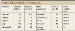
Current technologies such as Camera Link, USB 2.0, FireWire, and Gigabit Ethernet are capable of extreme data rates only with extreme difficulty and expense (see Table 1). The only true candidate for extremely fast data rates is Camera Link.
Total GigaOPS required for real-time processing of images varies from an average of seven operations per pixel per routine to 50 operations per pixel per routine on the high side and from 1000 MegaOPS for a 1000-frames/s small-format camera running a single low-ops routine, to 50-100 GigaOPS for a large-format sensor running a single high-ops routine at 240 frames/s.
High-speed CMOS sensors come in arrays from approximately 640 × 480 pixels to 2300 × 1700 pixels. The frame rates vary from 240 to 2000 frames/s. FastVision undertook a study of the average number of operations required by an average suite of imaging routines. The study revealed an average of seven operations per pixel per routine on the low side to 50 operations per pixel per routine on the high side. The results vary from 1000 MegaOps for a 1000-frames/s small-format (512) camera running a single low-ops routine, to 50-100 GigaOps for a large-format (2048) sensor running a single high-ops routine at 240 frames/s .
A total throughput of tens of GigaOps to hundreds of GigaOps results from scaling by the number of routines required by a typical imaging application. Such a computational throughput swamps conventional microprocessor solutions. Thus, to meet these high-performance requirements, engineers generally resort either to ASIC/FPGA technology or to an application-specific silicon processor. Data rates are so high that even if you deliver the data to a computer, it is probably not possible for a general-purpose low-cost computer to process data at these rates (greater than 1 Gbyte/s continuously).
POTENTIAL INTERFACES
Emerging technologies including InfiniBand, 10-Gig Ethernet (10GigE), and PCI Express can achieve 500 to 1000 Mbytes/s. All of these are high-speed serial buses that use the same physical layer currently run in the 2.5- to 3.2-GHz range. PCI Express and 10GigE are beginning to be widely adopted by major suppliers and vendors. In the near future, these interconnections will expand into the 3- to 10-GHz range (see Table 2).
10GigE is the intentionally broad-based IPv6 centric network and targets fast occidental deliveries of unspecified and mostly unstructured data from anybody to anyone. Delivery is “the best effort,” and any guarantees have to be grafted on top using additional protocol levels and repeat communications. The main advantage is widespread connectivity.
InfiniBand comes from the needs of cluster computing that are very sensitive to latency of data exchanges and synchronization. Reliability of data delivery is also paramount, since computer applications have a hard time dealing with corrupted or missing data. InfiniBand was motivated by an emerging need for a “computer room interconnect.” It is targeting blade servers with the emphasis on reliable data transfer among thousand of computer systems.
PCI Express is driven by a much more practical goal of the scalable high-speed data interconnect in PC systems. It concerns itself with seamless support for PCI legacy devices, high-bandwidth data transfers, and scalability. All of these interfaces are nonproprietary. The widespread adoption of any of these emerging interconnect technologies will enable camera makers to use them to provide sufficient bandwidth for the most demanding storage or postprocessing requirements.
The adoption of alternatives to Camera Link depends on the availability of a low-cost silicon implementation of the interface that can be used by camera or frame-grabber manufacturers or PC users. If or until this evolution occurs, the cheapest and fastest interface is Camera Link, especially in the mid-range market of less than 250-Mbyte/s data-transfer rates. This market includes most cameras currently produced, with the exception of the very-high-end cameras based on high-end sensors.
Dalsa, Waterloo, ON, Canada; www.dalsa.com
FastVision, Nashua, NH, USA; www.fast-vision.com
FillFactory, Mechelen, Belgium; www.fillfactory.com
Micron Technology, Boise, ID, USA; www.micron.com
JOSESPH SGRO is CEO and PAUL STANTON is vice president of FastVision, Nashua, NH, USA; www.fast-vision.com.


