PCI Express captures frame-grabber designs
New generation of boards will guarantee the bandwith demanded by multiple-camera configurations.
By Andrew Wilson, Editor
It has been more than two years since National Instruments announced the world’s first PCI Express frame-grabber boards. Since then, a number of other established companies have entered the market with products that enable system integrators to capture a variety of analog and digital signals.
For the most part, the increasing success of the PCI Express interface has been due to its ease of implementation over existing PCI and PCI-X designs, its high throughput, and the increasingly greater availability of compatible motherboards and peripheral cards. This year’s VISION Show, held earlier this month in Stuttgart, Germany, showed just how popular this new architecture has become with at least five companies adding to their portfolio of PCI Express products (see table).
For many developers of these peripheral products, the appeal of PCI Express comes from its scalability. Previous generations of PCI and PCI-X designs were parallel buses that used synchronously clocked data that could not easily be scaled in frequency. While the final incarnation of the bus, the 133-MHz PCI-X, could transfer data at a peak 64-bit transfer rate of 1 Gbyte/s, it has been surpassed by the performance benefits associated with PCI Express.
Point to point
Unlike the PCI bus, PCI Express is a serial point-to-point architecture. Because it is backwardly compatible with the PCI bus, existing applications written for PCI-based products are compatible. In its design, a pair of transceivers transfers data between the PCI Express interface on the add-in board and the PC. These LVDS signals can be scaled by adding signal pairs, resulting in x1, x4, x8, and x16 lane widths.
Once the two PCI interfaces at each end of the PCI Express link negotiate lane widths and frequency of operation, point-to-point data are then striped across the LVDS interface. While the PCI Express x1 link has a peak bandwidth of 2.5 Gbytes/s, an effective maximum bidirectional data-transfer rate of 5 Gbytes/s is possible. However, because the PCI Express architecture encodes 8-bit data bytes into 10-bit transmission characters using 8b/10b protocol, the effective bidirectional bandwidth is 80% of 5 Gbytes/s, or 4 Gbytes/s.
“Although the bandwidth of an x8 slot is 4 Gbytes/s,” says Reynold Dodson, president of Bitflow, “this is the total bidirectional bandwidth. In other words, each PCI Express lane is capable of moving 256 Mbytes/s of data in one direction and 256 Mbytes/s of data in the other direction. So the total bandwidth of one lane is 256 + 256 = 512 Mbytes/s. However, frame grabbers only send data in one direction to the host. So it is dishonest to quote the bidirectional bandwidth.”
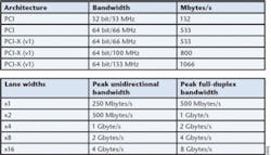
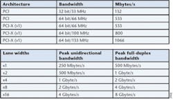
FIGURE 1. Comparing the bandwidth attainable using x1, x2, x4, x8, and x16 PCI Express implementations with PCI (64 bit/66 MHz) and PCI-X (64 bit/133 MHz) shows that the 533 Mbytes/s of the PCI-64 implementation is roughly comparable to that of an x2 PCI Express implementation (top). Similarly, the 1-Gbyte/s data rate of PCI-X is only matched by the performance of the x 4 PCI Express (bottom).
For designers of frame grabbers and digital interfaces, the x1, x4, x8, and x16 protocols create somewhat of a conundrum. Comparing the bandwidth attainable using x1, x2, x4, x8, and x16 PCI Express implementations with PCI (64 bit/66 MHz) and PCI-X (64 bit/133 MHz) is interesting (see Fig. 1). The 533 Mbytes/s of the PCI-64 implementation is roughly comparable to that of an x2 PCI Express implementation. Similarly, the 1-Gbyte/s data rate of PCI-X is only matched by the performance of the x4 PCI Express (seeVision Systems Design, August 2005, p. 37).
Click here to download a PDF of the table from page 96.
Most currently available PCI Express boards use the x1 configuration of the standard to offer a maximum 250-Mbytes/s peak unidirectional bandwidth between frame grabber and host CPU. In many cases, the x1 interface provides enough bandwidth. In the design of its PC-EYE Mono, for example, Eltec offers a frame grabber capable of supporting four multiplexed monochrome channels at a maximum data rate of 8 bit and 40 MHz/channel. This results in a maximum sustained bandwidth of 160 Mbytes/s, well within the performance specification of the x1 PCI bus specification.
FPGA support
To build such interfaces cost-effectively, designers can look to support from FPGA and off-the-shelf transceiver vendors. Recently, for example, Naseem Aslam, senior product marketing engineer of Altera, showed how a x1 interface could be constructed using the company’s Cyclone II FPGA and an external x1 PHY from Texas Instruments. “When FPGAs are already being used in a design and adding PCI Express functionality is desired, the FPGA and x1 PHY solution makes it simple to integrate the PCI Express,” he says (see “A low-cost solution for FPGA-based PCI Express implementation,” www.pldesignline.com).
“The big advantage with discrete PHYs from companies such as Genesys Logic America, Philips, and Texas Instruments [TI],” says Brian Daellenbach, president of Northwest Logic, “is that with a discrete PHY, low-cost FPGAs, such as Lattice’s ECP, can be used. And since the throughput obtainable between the discrete PHYs and PHYs that can be integrated onto high-performance FPGAs is approximately equivalent, there’s no reason to choose one approach or the other on a throughput basis.”
The advantage of using an integrated PHY is that it enables a more sophisticated design to be implemented, reduces FPGA pins and board space, and may generate a slightly higher performance solution. “Most people who are designing x1 implementations are typically using discrete PHYs with lower-cost FPGAs,” says Daellenbach.
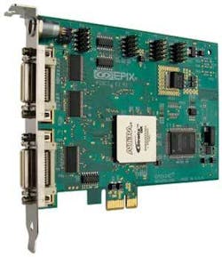
This is not the case, however, in the design of the latest x1 PCI Express frame grabber from Epix. Although company president A. C. Petersen declined to comment on the specifics behind the design, it appears that the board uses an Altera Stratix GX with integrated transceivers (see Fig. 2). In operation, the PIXCI E1DB Dual Base Camera Link board interfaces to one or two base configuration Camera Link cameras at sustained data-transfer rates to 204 Mbytes/s.
FIGURE 2. The latest x1 PCI Express frame grabber from Epix appears to use an Altera Stratix GX with integrated transceivers. The PIXCI E1DB Dual Base Camera Link board interfaces to one or two Base configuration Camera Link cameras at sustained data-transfer rates to 204 Mbytes/s.
“With x4 implementations, there are a relatively even mix of customers using both discrete PHYs and FPGAs and full FPGA implementations,” says Daellenbach, “and for x8 implementations, the majority of customers are using integrated PHYs.” While this may be true in markets other than machine vision, it appears that designers of frame grabbers have taken a somewhat more cautious approach.
Building bridges
Indeed, there are other ways to implement the PCI Express interface, especially when upgrading older PCI and PCI-X designs. To do so, many vendors, especially those building x4 PCI frame grabbers, are using bridge chips in their designs. Devices, such as Intel’s 41210 serial-to-parallel PCI Transparent Bridge chip, for example, can connect parallel bus PCI and PCI-X technology-based frame grabber card designs directly to the PCI Express’ serial I/O architecture.
Configured with an x4 or x8 lane upstream port connection to host PCI Express slots, the Intel 41210 provides two 133-MHz PCI-X bus segments (1 Gbyte/s each) for attaching legacy PCI and PCI-X designs behind the bridge. While these boards are not native PCI Express implementations, they do offer PCI Express compatibility and the high bandwidth/connector and the quality-of-service benefits of the standard.
“If Intel invented PCI Express, they should know how to make an interface,” says Avner Butnaru, CEO/chairman of Bitflow. In the design of the company’s first frame grabber, the R64e, Butnaru opted for the Intel Lanai (41210). “This PCI-E x8 bridge integrates the PHY and MAC in one off-the-shelf device,” he says.
For the company’s next-generation Karbon-CL frame grabber, Butnaru says, “We realized that an FPGA and an off-the-shelf core do not approach the Lanai in terms of both price and performance. Cores were mostly available in x1 and x4 formats and x8 cores required too much silicon. Having the PHY on the FPGA also increases the price of the FPGA dramatically.”
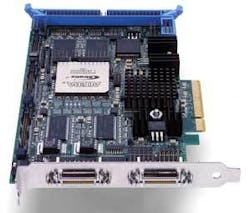
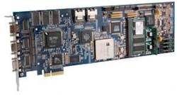
Because of this, the Karbon-CL also adopts the Lanai with the heart of the system implemented in an Altera Stratix. As a half-size x8 PCI Express implementation, the Karbon-CL is the world’s first four-camera Camera Link PCI Express frame grabber (see Fig. 3). It can acquire data simultaneously from up to four Base CL cameras or two Full CL cameras (including 10-tap Camera Link cameras) at 85-MHz pixel clock rates and can DMA data to the host at rates up to 2 Gbytes/s.
According to Butnaru, an advanced version of the Karbon (now under development) will operate in a stand-alone mode with on-chip operating system. To achieve this, Bitflow will use multiple NIOS DSPs implemented in the Stratix. To address less-complex applications, BitFlow also announced the Neon, a Base only PCI-E x4 lanes frame grabber, at VISION 2006.
Both Alacron and Matrox have also used bridge devices in their designs. For its part, Matrox has used such a device to implement a x4 PCI Express interface in the design of the its Solios eA, a frame grabber capable of simultaneously acquiring data from up to four single-output video sources. Alacron also uses a bridge chip in its Fast-Xe, a frame grabber that features no less than four GigE ports, three basic 85-MHz Camera Link channels, or an extended Camera Link camera interface, and an auxiliary I/O connector provides a header for adaptation of other high-speed interfaces.
Using an ExpressLane PEX 8114 bridge from PLX Technology, the device is equipped with a PCI Express port that scales to x1, x2, or x4 and a parallel bus segment supporting PCI-X or PCI operation. “In the Fast-Xe programmable frame grabber,” says Joseph Sgro, CEO of Alacron, an FPOA from MathStar serves as an application accelerator that is connected to the central data path by a cross-bar implemented in a Lattice FPGA” (see Fig. 4).
FIGURE 4. Alacron uses a bridge chip in its Fast-Xe-a frame grabber that features no less than four GigE ports and three basic 85-MHz Camera Link Channels. In the Fast-Xe design, an optional FPOA from MathStar serves as an application accelerator that is connected to the central data path by a cross-bar implemented in a Lattice FPGA.
The MathStar FPOA and its memory reside on a small mezzanine board and mate directly with the FPGA using a high-speed, 152-pin LVDS connector. Data preprocessed by the FPGA are passed to the FPOA for computation acceleration. “This is complemented by the DSP-processing power of the Stretch S5610,” says Sgro.
All onboard
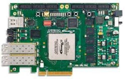
As indicated by Northwest Logic’s Daellenbach, however, high-performance, high-throughput digital Camera Link boards will eventually be integrated with FPGAs that provide designers with the PCI Express interface and other functionality. To rapidly implement these frame grabbers using their devices, FPGA vendors and their third parties are providing support. For its part, Altera’s PCI Express Development Kit, the Stratix II GX Edition, offers x1, x4, and x8 lane support (at 2.5 Gbytes/s per lane) using the company’s Stratix II GX FPGA (see Fig. 5). The board also features a 10/100/1000 Ethernet PHY (GMII) with RJ-45 (copper) connector, two SFP module interfaces (optics not included), 256-Mbyte DDR2 SDRAM, 2-Mbyte QDR2 SRAM, and 64-Mbyte Flash memory.
FIGURE 5. To rapidly develop frame grabbers, FPGA vendors such as Altera offer its PCI Express Development Kit, dubbed the Stratix II GX Edition. The board offers x1, x4, and x8 lane support (at 2.5 Gbits/s per lane) using the company’s Stratix II GX FPGA and features a 10/100/1000 Ethernet PHY (GMII) with RJ-45 (copper) connector, two SFP module interfaces, 256-Mbyte DDR2 SDRAM, 2-Mbyte QDR2 SRAM, and 64-Mbyte Flash memory.
PLD Applications takes the development process one step further by offering its PCIe Xpress GXII PCI Express development board that also features the Stratix II GX FPGA. First announced at this year’s NIWeek, PLD Applications’ optional Camera Link daughter card allows images from cameras such as Basler’s 48-frame/s A202k Base Camera Link camera to be captured and processed and transferred to a host CPU (seeVision Systems Design, October 2006, p. 45).
Plugging in
As the technology of PCI Express emerges and more frame grabbers become available, developers must be wary when choosing system motherboards in which to deploy them. Most motherboards support concurrent full DMA speed on all of their PCI Express slots. And an x8 board, for example, will work in not only x16 and x8 slots, but also, as is becoming the trend, x4 and x1 slots that use x16 connectors. Although performance will be degraded in these x1 and x4 slots if, for example, x8 boards are used, they will operate in applications that do not require the maximum transfer data rate.
“Some consumer motherboards, such as those using Intel 915, 925, and 954 chipsets, really only support the PCI Express bus for graphics cards,” says Bitflow’s Dodson. “If they see anything other than a VGA in the x16 slot, they switch the slot to x1 mode, reducing the performance of the system. At present, we do not recommend motherboards using these chipsets for machine-vision applications, although these problems may be fixed by BIOS updates or changes in the design of the motherboard.”
Some frame-grabber vendors offer a list of motherboards and even “blog-like” postings that recommend specific motherboards that fully support the PCI Express interface.
null
