Integration Insights: CMOS imagers target high-speed applications
Higher frame rate CMOS imagers enable multiple exposure wide dynamic range for intelligent transportation applications.
Arnaud Destruels
It's safe to say that there has been an unrelenting focus on production line efficiency-be it in traditional sectors, or even in ones that rely on excellence and craftsmanship such as the luxury watch industry. Machine vision has proved pivotal in enabling this, but challenges are getting ever harder.
To meet these demands, and continue to improve both productivity and quality, industrial vision systems will again need to make a big leap. If we look at systems like robotic production lines, these are now able to build even highly complex products, and do so at exceptionally high speed.
One sector that typifies this well is PCB assembly, for example, with SMT placement equipment (more commonly known as chip shooters) able to place parts at a rate greater than 30 per second - that's over 100,000 per hour.
Placement accuracy is, therefore, of great concern, with careful inspection being essential in ensuring PCBs that have incorrectly mounted components are spotted and stopped before they enter final assembly.
Additionally, it's vital that errors are spotted as quickly as possible to prevent wastage from other components being mounted on a board already outside of tolerance.
It is therefore essential to adopt machine vision systems on a line, as well as full-board inspection systems between assembly stages. This need is even greater when high pin-count or high-cost components are involved.
As such, systems with high frame rate cameras and with communication interfaces capable of high-data transfer rates have become essential-ensuring full resolution images are sent continuously for rapid processing.
But that's not the whole story behind speed.
Lighting
Lighting's role in effective industrial image processing is vital. Illumination (via LED or other light source) needs to be high enough in the area of interest to minimize the camera's exposure time.
Furthermore, its direction must be highly controlled in order to create a high contrast and allow key features to be recognized and read against their background.
And similarly, uniformity plays a vital part in reducing the amount of post-processing time needed by the software in order to detect each mounted component.
However, it's rarely as easy as it sounds. Some of the main challenges come when parts of the sub-assembly being captured lie in the shadow of larger components or when the bright lighting that allows you to capture images of parts effectively when they have low contrast against the substrate, lead to glare in other parts of the image.
Back end processing / wide dynamic range
These issues can, to a greater or smaller extent, be managed by employing image processing, run on the back-end computer system. But this requires compromises in order to enable the board to be captured in one image-and the ultimate effect on this is that accuracy may be sacrificed
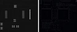
Here, the higher frame rates that are enabled by CMOS imagers enables you to overcome this problem and achieve an illumination consistency-via a process called wide dynamic range (Figure 1). The technique takes multiple shots in sequence, each with a slightly different exposure time.
By combining these and creating a composite photograph you can achieve a much higher bit depth than a single image. And the end result is that shading on parts of the image is corrected without the loss of effective bit depth that would be seen with a single-exposure.
Similarly, using multiple captures and creating a composite image will also increase the overall image quality. For example, heat haze can cause different parts of each subsequent image to be slightly blurred, making it harder for the image processing software to spot problems or cause it to fail a perfectly valid product-which would then need either re-inspection or would be scrapped, expensively.
By taking an image average, it enables image defects to be removed quickly and effectively, meaning only real issues are flagged.
The use of WDR and image averaging (often referred to as multi-pixel averaging) provides key features that can be used in outdoor applications-in particular for intelligent transportation systems (ITS). Here, the quality of light varies significantly-for example the low sun in winter gives huge differences in the light levels for number plate recognition systems. WDR makes it possible to read number plates, not just when the light levels are unpredictable, but also when they change rapidly-for example when shading from an overtaking vehicle masks all or part of the number plate.
The rise of CMOS over CCD imaging technologies
The evolution of CMOS sensors has meant machine vision systems can now manage the intense requirements that are dictated by high-throughput capture and of multiple-image capture. In contrast to traditional imagers, based on the charge-coupled device (CCD) architecture, CMOS imagers are able to leverage massive parallelism.
A CCD sensor uses a long-shift register in order to read the pixels in series. This is a significant rate-limiting step and acts as a bottleneck, slowing throughput. Conversely, a CMOS imager can place an A/D converter at the end of each pix row.
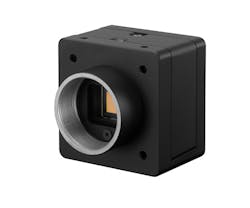
This allows the output registers to simultaneously collect image information from an entire column of converters-as an example, the latest generation of Sony's Global Shutter (GS) CMOS imagers delivers frame rates up to 150 fps, at resolutions of 5 megapixels (Figure 2). This is an order of magnitude quicker than a comparable resolution image from a CCD sensor.
Using such a high-frame-rate camera gives this headroom and enables multiple-exposure WDR as well as defect-removal techniques.
Global shutters improve accuracy
Accuracy can be further enhanced by the use of a global shutter. These ensure the exposure for all pixels within an image happens at the same point in time, unlike for less-optimized rolling-shutter architectures.
When used to capture images on high-speed production lines, these rolling-shutter architectures create errors as a result of each row of pixels being exposed and captured in series, while this has no effect for standard uses, objects moving at speed will highlight the fact that each row is captured at a slightly different point in time, creating distorted images from the camera.
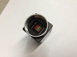
The improved spatial accuracy also reduces the burden placed on the image processing hardware as it reduces the chance of mis-recognition and then eliminates the requirement to undertake translation or rotation corrections on the outputted raw images. The GS CMOS, for example, further improves this through a design with extremely fine tolerances on the mounting points (Figure 3).
The need for synchronization
Because of these high frame rates, there is now a need to synchronize in time systems on the production line (or those used by applications such as ITS) using the IEEE 1588 Precision Time Protocol (PTP). This synchronization of systems on a network (e.g. a GigE network) to a common clock through PTP allows an object in any given frame to be easily, precisely and quickly identified for removal (or remedial processing) further downstream by the production line's robotic systems.
Communication standards
There are several communication standards used in machine vision, such as GigE, Camera Link, etc. To maximize the speed (throughput) via these interfaces, especially on multi-camera systems, it is vital to avoid packet collisions and bottlenecks that result from changing network conditions. Features such as intelligent flow control, which can be found on today's advanced imagers-such as the GS CMOS, help to better manage this process.
Conclusion
The machine vision industry has helped countless sectors continue to improve efficiencies. Processor speeds and sensor technologies will continue to improve at a rapid rate, but a high-quality, highly-efficient system is about more than just these features.
A holistic approach to system design is needed; to use a sports analogy, we need to continually make marginal gains to cut each bottleneck, and through this approach we yield a camera architecture that provides a wide variety of industries with the ability to accelerate their processes, and provide the efficiency gains to their customers.
Arnaud Destruels, VC Product Marketing Manager, Sony Image Sensing Solution Europe, Weybridge, Surrey, United Kingdom (www.image-sensing-solutions.eu)


