Vision system aligns laser diodes precisely
By Jeff Child,Contributing Editor
Attaching very small laser diodes on top of semiconductor circuits is a key step in the creation of fiberoptic and optoelectronic devices. Common devices in that category include source lasers and pump lasers. Source lasers generate digital pulses that travel along the core of fiberoptic cables. Pump lasers are used in equipment that amplifies those digital signals as they're sent over long-haul transmission networks.
Making these devices involves accuracy and complexities a level above those of typical electronic-component-assembly processes. When a simple component such as a capacitor, for example, is placed on a semiconductor substrate, the capacitor tends to function correctly as long as its leads are properly connected to the circuit. In contrast, a laser diode must be placed at a precise position and orientation or it won't work. This is because laser diodes are extremely sensitive to temperature variations. Placing them incorrectly on a semiconductor substrate can put them too near to current flows, thereby distorting their proper operating temperature and function.
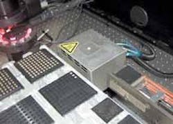
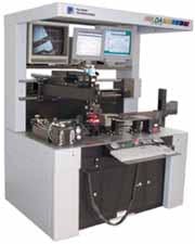
Palomar Technologies (Vista, CA), a manufacturer of component assembly equipment, faced such challenges when crafting its laser-diode-assembly (LDA) system. The system incorporates a gray-scale pattern-recognition vision system to precisely place randomly oriented laser diodes under a variety of background and lighting conditions (see Fig. 1).
In addition to temperature sensitivity, other factors make laser-based device assembly a challenging task. Today's semiconductor laser diodes are as small as 10 x 10 mil. This small size combined with increasing power densities, approaching 400 mW, creates power-dissipation issues. "If you do the math, that's the equivalent of trying to dissipate the entire heat of a 40-W light bulb through the tip of your little finger," says Ed Wills, product marketing manager for component assembly systems at Palomar Technologies.
Consequently, the bond that attaches the bottom of the laser die to the gold pad on which it rests must dissipate that heat. To do so effectively, the bond must provide a complete, uniform, and void-free interface. Otherwise, the heat could damage the laser. Further complicating matters is the wide variation among laser modules fabricated by various manufacturers. "You could have two separate manufacturers who build a module that performs the same end-user function. They'll use different methods to assemble it, and the part will look completely different," says Wills. "Those variations must be overcome through creative application techniques, as well as some adjustments with the integrated vision system."
Wills also remarks that there's so much secrecy between laser vendors that there's no consensus about what a good laser should look like, how it should be bonded, and how it should be presented. As a result, the Palomar LDA system is designed to accommodate a range of variations.
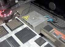
The basic function of the LDA system is to place small laser diodes onto larger substrates using a eutectic solder die-bond process (see Fig. 2). The assembly system integrates a Cognex (Natick, MA) 5400 series intelligent frame grabber into a slot-card industrial PC that forms a vision system used at multiple points in the assembly process. The assembly system places the laser on top of a slightly smaller piece of solder. The vision system applies a pattern-recognition algorithm to locate either the corners or the edges of the die. Using the imaging data, the bond head picks and places the die and positions it on the substrate so that it rests on a heating stage.
The vision system performs another pattern-recognition routine on the substrate to target the bond pad on which the laser die is placed. At that point, the bond head places the die, holds it in place, and then triggers a heat pulse according to the proper profile. The die is held in place with typically less than 30 grams of force. The laser is held in place while the assembly system melts the solder. Then, the solder cools and solidifies. After this process is completed, a postplacement accuracy check can be done with the vision system if required. The LDA system is capable of placing multiple lasers on a die, although most applications use just one per subassembly.
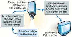
The vision system uses a Panasonic Security & Digital Imaging Co. (Secaucus, NJ) 1/2-in. CCD camera with a resolution of 800 x 600 pixels. To accommodate the wide variations in laser configurations, the vision system is set up to support about 20 interchangeable lenses, two of which can be mounted on the bond head. High- and low-magnification options are available, depending on the type of laser die under scan. The camera is supported by on- and off-axis lighting clusters that illuminate the bond-pad metallization or highlight the surface features, depending on requirements. The frame-grabber card handles all the vision specifications used to accept or reject a part (see Fig. 3).
Timing is critical in the LDA system because its integrated vision system performs image-capture processing at multiple steps in the assembly process. These requirements determined the selection of the smart 5400 frame-grabber board.
All vision processing occurs independently on the frame-grabber board, minimizing bus traffic and reducing the workload of the host-system processor. The 5400 board operates completely stand-alone within the host PC and draws only power from its backplane.
Software engineers at Palomar developed the bulk of the application and user interface software in the LDA system by incorporating elements of Cognex vision libraries. The application runs on a host PC system running the Microsoft (Redmond, WA) Windows operating system. Cognex engineers assisted the Palomar engineers in the design of the LDA lighting and imaging systems.
A key aspect of Palomar's design strategy was to craft the LDA system to be future-proof. This allows for easy upgrades to advances in vision-system technology. It also accommodates numerous changes by the user. In markets such as fiberoptics, performance specifications change rapidly. This market, while currently in an economic slump, has seen boom times in the past and is expected soon to receive huge ramp-up orders.
When this market is accelerating, laser subsystem manufacturers are forced to buy laser diodes from multiple suppliers. The resulting problem is that no two suppliers produce the exact same parts. Moreover, parts are diced slightly differently or contain slightly different cleave angles. All these factors call for more advanced vision technology to accommodate the variations in parts while maintaining assembly accuracy.
With the increasing capabilities of faster processors, Palomar designers anticipate that future versions of its LDA system could move to using a dumb frame-grabber board and shifting the image-processing burden onto the host CPU. On the software side, Palomar developers see production benefits in moving to more advanced pattern-matching schemes. These schemes should enable the LDA system to do a single-point capture, thereby saving a movement step on the bond head and increasing overall throughput.
Enhanced pattern-matching schemes should help the LDA achieve greater q accuracy; q is the angle of the die being placed. "That's important because you need to align the emitting access of the laser with the components in the optical train, such as the lenses, fiber, and rear facet monitor," says Wills, "In the surface-mount industry, just dropping a die into its hole is sufficient. But in the optics industry, the x, y, and q specifications must be correct. If you hang the laser over the edge of the bond pad, it could burn due to a lack of sufficient heat transfer. And you must have ( in line because, if the laser die is placed crooked, the process is useless. It's like having the headlights of your car pointed 30° to the side," he adds.
Other benefits expected to be gained by moving to enhanced pattern recognition include a possible slight reduction in camera magnification. Because the LDA system is essentially aligning die in multiple dimensions, a number of depth-of-field issues cause confusion. Even when a die is in focus the part can still appear to look different. More advanced pattern recognition can help reduce depth-of-field problems by keeping patterns consistent.
Company InformationCognex Corp.Natick, MA 01760Web: www.cognex.comMicrosoft Corp.
Redmond, WA 98052
Web: www.microsoft.com
Palomar Technologies
Vista, CA 92083
Web: www.palomartechnologies.com
Panasonic Security & Digital Imaging Co.
Secaucus, NJ 07094
Web: www.panasonic.com/mv


