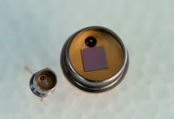
Jenoptik photodiodes for photometric applications do not require an additional filter
Selective photodiodes with angle-independent response spectrum detect a predefined wavelength range without the need for inserting additional filters, unlike conventional silicon photodiodes. The miniaturized diodes provide spectral receiving characteristics that are independent of the radiationangle of incidence. They are suitable for photometric applications with space-constrained systems in which an extended measurement range (dynamic range) is needed. Materials of manufacture include GaP, AlGaN, AlGaAs, InGaAs, or SiC and the devices are designed for a spectral range of 150 to 1750 nm; housed in hermetically sealed packages they are thermally stable up to 125°C.
Jenoptik Optical Systems Division
Jena, Germany
-- Posted byVision Systems Design
View More Vision+Automation Products
Locate a vendor or system integrator in our Online Buyer's Guide
---
NEW PRODUCT PRESS RELEASE
Jenoptik at electronica in Munich with New Photodiodes and Increased Assembly and Packaging Technology up to 300 millimeters wafer size.
Selective Photodiodes with Angle-Independent Response Spectrum
Jenoptik has developed a new product range of photodiodes with an angle-independent response spectrum. Compared with conventional silicon photodiodes, the new photodiodes detect a predefined wavelength range without the need for the insertion of an additional filter. Unlike dielectric filters, they also provide spectral receiving characteristics that are independent of the angle of incidence of the radiation.
The new photodiodes are ideally suited for all photometric applications where an extended measurement range (dynamic range) is required. These new space saving wavelength-selective radiation detection diodes can now be achieved space saving and follow the trend towards miniaturization while simplifying assembly.
Jenoptik provides customer specific solutions and a wide range of photodiode products as preassembled standard products in SMD and TO housings. The photodiodes are made from materials such as GaP, AlGaN, AlGaAs, InGaAs, or SiC and are designed for a spectral range of 150 to 1750 nanometers. Their detection is wavelength-selective, and they are characterized by their excellent signal and noise performance. In hermetically sealed special housings they are thermally stable up to 125°C.
Photodiodes provide safety. They are widely-used in Automotive, Security and Health Care industries in a wide range of applications including daylight/tunnel sensors or lane departure warning systems in vehicles, in monitoring safety levels in gas detectors, in water disinfection for monitoring dosages of UV radiation, as flame sensors for burner monitoring, as detectors in photoelectric sensors, and for analysis of body fluids concentration in medical technology.
Extended Assembly and Packaging Process for Customized Image Sensors
Jenoptik has extended the Assembly and Packaging process chain by recent investments in wafer sawing and multi-chip bonding, up to 300 millimeters wafer size manufacturing. This enables customers to realize economical solutions with high-precision production processes that are at the forefront of technology. The new systems are particularly suitable for the processing of complex customized micro-electronic components such as image processing sensors.
Using the more powerful double-spindle wafer saw, it is now possible to process wafers of up to 300 millimeters in diameter. The new fully automatic system cuts, cleans and exposes the wafers contained in a magazine. The two-spindle saw also reduces the cycle time by more than half when compared to the semi-automatic processes. Its intelligent water supply system makes the saw especially suitable for the processing of silicon-based image sensors and optical glass.
Jenoptik now works with a multi-chip bonder to further process the 300 millimeter wafers. Depending on the quality of the source material, this chip bonder achieves a placement accuracy of up to ±10 microns and can process chips with an edge length of between 0.2 and 80 millimeters.
The significant advantage of 300 millimeter wafer source material is that there is geometrically less waste. Depending on the chip size required, there is a correspondingly higher yield per wafer. This substantially reduces manufacturing costs for semiconductor chips in comparison with smaller wafer diameters.
Jenoptik has exhibited examples of products at its booth at the electronica trade fair to give visitors an idea of Jenoptik´s capabilities. These exhibitions range from the basic wafer material to the complete micro-electronic component, including software. Furthermore, the company demonstrates its expertise in digital image processing, from application-specific CMOS imaging modules to microscope cameras from the ProgRes® range and options for integrated, customized image-processing systems.
About the Jenoptik-Business Unit Optoelectronic Systems
The Optoelectronic Systems business unit is a provider of integrated optoelectronic system solutions. The business unit has expertise in the development of optics, electronics and software and in manufacturing technologies for the production of polymer-based optical and electronic components and modules as well as in the assembly of entire devices. All important value adding stages for system integration can be implemented by the Optoelectronic Systems business unit from development and design to prototype manufacturing, supply chain management and series production.
Through its Optical Systems division, the Jenoptik Group delivers world class precision optics and systems designed and manufactured to the highest quality standards.
Besides offering customized systems, modules and assemblies, the Optical Systems division is a development and production partner for optical, microoptical and coated optical components - made of optical glasses, IR materials as well as polymers. It possesses outstanding expertise in the development and manufacture of optics and microoptics for beam shaping used in the semiconductor industry and laser material processing.
The product portfolio also includes optical and opto-electronic systems and components for applications in defense & security, health care & life science, digital imaging, machine vision as well as lighting.
Contact
Mario Schmidt
Sales
JENOPTIK Polymer Systems GmbH
Koepenicker Strasse 325b, Haus 201
12555 Berlin I Germany
Telefon: +49 (0)3065 7625-09 I Fax -45
[email protected]
SOURCE:Jenoptik Optical Systems
