IMAGE PROCESSING: Third parties add vision modules to PXI systems
For point and neighborhood image-processing algorithms, leveraging the power of the parallelism found in FPGAs can be beneficial. Because the devices inherently support a data-flow architecture, they can be used to support real-time preprocessing functions such as image thresholding and filtering, color correction, and flat field correction. Consequently, most camera and frame grabber companies currently employ these devices to perform either limited preprocessing algorithms within the camera itself or complete tool kits that allow the user to program the FPGA directly on the frame grabber.
To effectively program devices, however, still requires an intimate knowledge of the device architecture since the developer must fully understand the timing, triggering, and synchronization of data and the on-board memory and functionality of the device.
To ease the design process, companies such as National Instruments (NI; Austin, TX, USA; www.ni.com) have taken a more graphical approach, producing add-in boards and associated software. In the development of its FlexRIO product family, for example, NI offers a PXI-based add-in board known as the FlexRIO FPGA module, which contains a Xilinx Virtex-5 FPGA and a number of adapter modules that interface directly to the front of the board to provide direct I/O capability.
To program this FPGA board, developers can use the company’s LabVIEW programming language to program the FPGA with a LabVIEW block diagram. By using code generation techniques, this LabVIEW graphical development environment is then synthesized to FPGA hardware.
To support the FPGA board, NI has released a number of adapter modules for its FlexRIO FPGA module including a 3-GS/s, 8-bit digitizer for time-domain measurements; a four-channel, 250-MS/s, 14-bit digitizer; and a Camera Link interface that allows Base, Medium, and Full Camera Link cameras to be interfaced to the FlexRIO FPGA module.
At NIWeek 2009, NI demonstrated its Camera Link adapter module in conjunction with a 10-tap A504k Camera Link camera from Basler Vision Technologies (Ahrensburg, Germany; www.baslerweb.com). With a 1280 × 1024-pixel progressive scan CMOS array clocked at 67 MHz, the 10-tap A504k camera can capture 500 frames/s and transfer this data directly to the FPGA on-board the FlexRIO FPGA module for high-speed, low-latency laser tracking. The image acquisition, preprocessing, centroid measurements, and laser control all take place inside the FPGA.
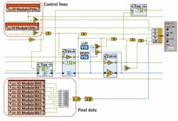
To ease programming of image data using the FPGA, NI has developed LabVIEW virtual instruments (VIs) that graphically show the data path, frame, data valid, and clock signals from the adapter board to the FPGA (see Fig. 1). In this way, the developer can define signals from the camera and how the data is captured by the FlexRIO FPGA module into the board’s 256-Mbyte DRAM and processed by the FPGA.
In a presentation, Brent Runnels at NI showed how using this software developers could implement FPGA functions such as pixel processing, image thresholding, image filtering, and centroid analysis. To extend this concept further, the company has set up an IP repository called IPNet, where developers can share LabVIEW FPGA IP blocks or submit updates to existing IP. Extending the concept further, NI is encouraging third-party vendors to develop their own adapter modules for FlexRIO.
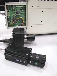
At NIWeek, for example, Averna (Montreal, QC, Canada; www.averna.com), showed an IEEE 1394b adapter module with three independent IEEE 1394b ports. Not to be outdone, Adsys Controls (Irvine, CA, USA; www.adsyscontrols.com) showed its own combined Camera Link and GigE Vision adapter module for the FlexRIO FPGA, dubbed ProLight CLG-1. Like the NI adapter module, the board can support Base, Medium, and Full Camera Link configurations as well as a GigE interface (see Fig. 2).
According to Brian Goldberg, president of Adsys Controls, the board can also support one Camera Link camera and a GigE camera running simultaneously. The GigE interface allows a high speed external communication interface that can be configured by the user for such things as piping full frame data out directly from the FPGA to a data recorder. To support clock triggering or custom programmed I/O, the board features four digital I/O lines that can be used for triggering and the module can also be configured for IRIG-B input for time synchronization. A Camera Link-only version of the ProLight board will be available October 2009.
While adapters, FPGA modules, and graphical system design software like these may be elegant, the pricing of these products is still rather high. However, NI does not appear to be concerned, for now. Rather, it will leverage its hardware and software solutions to third-party developers who require a simpler way of programming FPGAs than developing VHDL code.


