System tests CMOS imagers and cameras
Andrew Wilson, Editor, [email protected]
CMOS imagers from vendors such as Kodak (Rochester, NY, USA; www.kodak.com), Micron Technology (Boise, ID, USA; www.micron.com), and Omnivision (Sunnyvale, CA, USA; www.ovt.com) are being used in an ever-increasing range of end-user products. Before such devices and the camera modules based around them can be shipped, however, they must be tested at every stage of product development.
“Currently,” says Martin Vasey, CEO of Jova Solutions (San Francisco, CA, USA; www.jovasolutions.com), “three approaches are used to test these devices and systems. Large-volume image-sensor and camera-module manufacturers sometimesuse expensive automated production test equipment from Teradyne (Boston, MA, USA; www.teradyne.com) and Agilent (Palo Alto, CA, USA; www.agilent.com); however, it takes very large volumes to justify the high price of this approach. Smaller-volume sensor and camera-module manufacturers may simply use the evaluation boards provided by image-sensor vendors with which to qualify their imagers.
“The problem some companies experience using these evaluation boards,” says Vasey, “is that they are specific to each vendor. Each time a new device type needs to be evaluated, a new evaluation board must be purchased. Worse, such evaluation boards offer very limited evaluation functionality. Often, they provide no way to perform current measurement, control the device’s power supply, or provide timer/counter functionality. To properly evaluate such devices, test engineers can, of course, develop their own test rigs.”
“Generally,” continues Vasey, “these consist of off-the-shelf instruments such as frame grabbers, power supplies, oscilloscopes, custom-designed testbeds, and sophisticated image-analysis algorithms to evaluate the ICs and the camera modules built around them. Developing these systems requires a high level of expertise and can take many man-months and cost tens of thousands of dollars.”
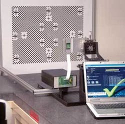
Design and test engineers no longer need to face this problem when evaluating CMOS imagers. Jova Solutions has developed a CMOS image-sensor and camera-module test station, the Image Sensor Lab ISL-1600, that provides a range of CMOS image-sensor interfaces and control, test, evaluation, and comparison capabilities and costs less than $5000. In essence, the ISL-1600 provides a bridge between the image sensor or camera module under test and a host PC that runs the unit’s software suite (see Fig. 1). This alleviates the need for test engineers to design and build their own test station using off-the-shelf power supplies, timer/counters, DMMs, interface controllers, and frame grabbers.

To interface to image sensors or camera modules, a simple adaptor makes the connections between the ISL-1600 standard connector pinout to the camera module’s specific mating connector and pinout. Jova Solutions makes custom adaptors to meet customer-specific requirements. A reference-adaptor template is provided free of charge so that customers can develop their own custom adapters quickly and cost-effectively.
According to Vasey, the company has developed more than 20 such boards for various semiconductor and camera vendors including Aurora Optical (Tucson, AZ, USA; www.aurora-optical.com), Exbiblio (Seattle, WA, USA; exbiblio.com), and Flextronics (Singapore; www.flextronics.com). “The interface boards generally cost between $800 and $1500 to develop, depending on the complexity of the imaging device or camera module. For devices Jova has already developed, this cost can be as low as $125,” says Vasey.
In addition to offering up to five user-selectable power supplies, I2C, and serial peripheral interface sensor communications and digital image-capture electronics, additional digital I/O lines support digital image sensor control and status lines such as reset, standby, LED, and flash. With a programmable on-board oscillator that provides master clock frequencies up to 136 MHz, image data are read from the CMOS image sensor or camera module using a 16-bit-wide data bus into the system’s 32 Mbytes of on-board memory.
The ISL-1600 can be interfaced to most CMOS imagers. Since the maximum data clock frequency of the unit is 136 MHz and data are clocked over a maximum 16-bit-wide data bus, the test unit cannot be used to test high-speed, multiple-tap image sensors. In fact, Jova Solutions is firmly targeting the CMOS imager and camera-module test market for its product.
“The ISL-1600 was designed as a generic sensor interface for bit parallel devices, and we’ve had great success interfacing to the devices our customers have,” says Vasey.A comprehensive software suite is supplied with the unit. Running on a host PC interfaced to the ISL-1600 over a USB 2.0 HI-SPEED bus, Jova Solutions’ Image Sensor Lab application software includes many of the common high-level characterization tests typically performed on image sensors during manufacturing or verification testing. These include photoresponse uniformity, dead- and defective-pixel detection, Macbeth color analysis, and MTF/SFR image-sharpness measurements.
“Image Sensor Lab also includes a scripting and sequencing engine that helps automate complicated startup and configuration procedures,” says Vasey. While script files are supplied for the more popular image sensors, new scripts can be developed using a simple text-based scripting language. The combination of hardware and software of the test system allows both image sensors and image camera modules to be tested.
“In most cases,” says Vasey, “the images generated from a CMOS imager will be very different from those from a camera module that uses the same semiconductor device.” One of these effects, for example, is lens vignetting, or “shading,” which describes the light fall-off observed toward the edges of an image.
“One of the tests incorporated into the ISL-1600 software suite,” explains Vasey “is the Bayer photoresponse uniformity algorithm. This calculates the mean and standard deviation of all the pixel intensities in the entire image, for each of the four Bayer color planes. To help eliminate lens-shading effects when using this test as a measure of the pixel noise in the image, an optional background-subtraction image-processing step can be selected.

The correction algorithm uses an nth-order filter and has user-configurable kernel size and percentile threshold algorithm inputs. The algorithm also calculates maximum neighbor nonuniformity across a user-specified grid of cells, returning the results as a maximum percentage deviation. Individual Bayer color planes can also be displayed as well as 3-D views of both the captured image-pixel intensities and the percentage deviation data (see Fig. 2).
Other tests include focus accuracy, spatial-frequency response/modulation-transfer function, dust and particle detection, and luminance uniformity, all of which are described on the company’s Web site.