Novel Sensors Help Smart Cameras Serve Niches
Andrew Wilson, Editor
Smart camera vendors now offer a number of products that target applications ranging from barcode reading to packaging inspection. These cameras generally employ off-the-shelf image sensors coupled with on-board processing and I/O capability. While typical smart cameras address multiple visible-light applications, more sophisticated camera designs are now emerging that address specialized niche applications such as fingerprint analysis, 3-D imaging, and nondestructive testing.
"Smart imagers" and the cameras that employ them use novel optics, filters, and sensors. Certainly, the concept of adding specialized technologies to sensors is not new. In 1976, for example, Bryce Bayer (then at Eastman Kodak) patented an RGB color filter array that mimics the physiology of the human eye. Now typically referred to as the Bayer pattern, the filter is commonplace in nearly every CCD and CMOS image sensor available today.
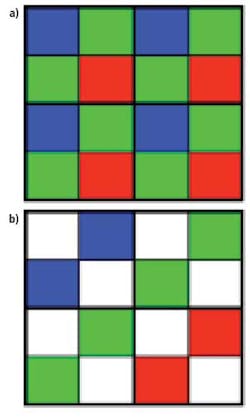
The Bayer pattern represents just one of the many methods that can be used to reconstruct color images. Two years ago, for example, Kodak Image Sensor Solutions (now Truesense Imaging) announced a variation of the Bayer filter pattern dubbed the Truesense color filter pattern. Developed by John Compton and John Hamilton of Kodak, the filter adds panchromatic pixels to the red, green, and blue elements that form the image sensor array (see Fig. 1).
Since the panchromatic pixels are sensitive to all wavelengths of visible light, they collect a higher proportion of the light striking the sensor. Using this method, Kodak claims that sensors such as the 1920 × 1080-pixel KAI-02150 that employ the filter are 2× to 4× more light-sensitive than those that use a standard Bayer color filter.
Of course, this increase in light sensitivity is traded for the resultant lower resolution of color pixels that can be resolved using demosaicing algorithms. Thus, cameras that use Truesense devices will probably likely find applications in traffic monitoring and surveillance applications, while those that employ the Bayer pattern will remain the choice of machine-vision camera developers.
Whatever type of filter pattern is employed, the resultant demosaicing that is required results in a color image that is of lower resolution than a similar image obtained by an equivalent monochrome sensor.
Because of this, developers of image sensors have looked for methods to capture multiple wavelengths at individual pixel sites. Perhaps the most publicized of these is the X3 series of imagers developed by Foveon, now part of Sigma Corp. Each pixel site on the imager is composed of three active pixel sensors that absorb different wavelengths of light at different depths.
Unlike monochrome image sensors that incorporate the Bayer pattern to produce color images, X3 sensors require no such filter. To date, the X3 sensor is being used in a number of Sigma's digital consumer cameras and specialized products such as the Toshiba Teli CSF5M7C3L18M camera that uses the Foveon X3 1/3-in. CMOS progressive-scan imager to render 1440 × 1080-pixel color images.
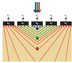
Just as the Foveon X3 exploits the differences in the semiconductor light absorption at different wavelengths, so too does the Transverse Field Detector (TFD), a color imager developed by Giacomo Langfelder, PhD, of the Politecnico di Milano. This imager relies on the creation of transverse electric fields such that charges generated at different depths in the silicon are collected by different surface contacts. In this way, three or more different spectral responses can be obtained without a color filter (see Fig. 2).
Polarized imagers
While traditional color imagers capture color and intensity, the third property of light—polarization—has been largely ignored by sensor and camera vendors until now. According to Viktor Gruev of the Computer Science and Engineering Department of Washington University in St. Louis, MO, polarization-contrast imaging is useful in applications such as target contrast enhancement in hazy conditions, underwater imaging, and noncontact fingerprint detection.
To measure polarization, Gruev and his colleagues have developed an imager that integrates silicon photodetectors and polarization filters on the same substrate. Incoming light is then filtered with spatially distributed micropolarization filters over neighborhoods of pixels, the amplitude of the light recorded by the photodetectors and the polarization computed (see http://bit.ly/HmVFxq).
Gruev is not alone in his endeavors. At the Fraunhofer Institute for Integrated Circuits, researchers have developed a camera based on the same concept that uses a conventional 1120 × 512-pixel CMOS image sensor overlaid with a 2 × 2 matrix of polarizing filters. This results in a camera with a 560 × 256 super-pixel imager that can be used to directly measure the polarization associated with the stress of an object (see "Smart camera measures stress in plastics and glass," Vision Systems Design, January 2012).
Smart optics
Just as integrating novel filters onto image sensors will widen the applications of such devices, so too will the addition of smart optics. These types of smart optics are now appearing in imagers targeted at specific applications such as hyperspectral imaging and close-contact applications such as fingerprint detection.
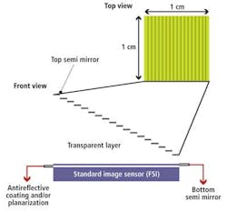
Most of today's hyperspectral imaging systems use dispersive light elements such as gratings and prisms in their designs, making them costly and bulky. To reduce this cost, researchers at IMEC have developed a means of producing the systems by integrating novel optics onto a standard CMOS imager (see "Novel technology lowers the cost of hyperspectral imaging," Vision Systems Design, January 2011).
In the design, a wedge of Fabry-Pérot filters is placed onto the imager so each filter will transmit a narrow band of wavelengths and reject wavelengths outside of that band (see Fig. 3). According to Murali Jayapala of IMEC's NVISION imaging program, this filter has been incorporated onto a 4-Mpixel image sensor to produce a prototype multispectral camera that transmits 100 spectral bands of 5-nm bandwidth at rates of 25 frames/sec.
Specialized optics have also been incorporated into a close-contact imaging system by Andreas Brückner and his colleagues at the Fraunhofer Institute for Applied Optics and Precision Engineering. The system, which integrates a microlens array with an off-the-shelf image sensor, achieves a resolution of approximately 3000 dpi across a 36.1 × 24-mm array with object-to-image distances as short as 5.3 mm (see "Microlenses make miniaturized closeup imaging a reality," Vision Systems Design, February 2012). Both the micro-optic and image sensor assembly have been integrated in a modified GE4900, 4872 × 3248-pixel CCD camera from Allied Vision Technologies.
Pixel shifting
The incorporation of micromechanical devices is also enabling specialized cameras to target niche markets. In microscopy applications, for example, it may be necessary to obtain very high-resolution images. To achieve the resolution, camera manufacturers are incorporating micromechanical stages into their cameras. In a technique known as pixel shifting, stages move the sensor a fraction of a pixel in the X and Y directions between each image capture. This results in a large amount of overlap between neighboring pixels for each image captured. Knowing the precise location of each sub-pixel shift, objects much smaller than the size of an individual pixel can be resolved.
One of the first companies to introduce this technology, Lumenera has developed a white paper that explains the technique in detail (http://bit.ly/HwZyQz). In its InfinityX32 camera, the company uses a standard 1616 × 1216-pixel, 4.4-µm2 pixel imager from Sony, coupled with the pixel-shifting technology, to obtain images of 32 Mpixels.
While Lumenera's technology remains proprietary, other vendors such as Olympus and Vieworks also offer this technique in their range of products. Olympus's DP73 uses a 2.1-Mpixel CCD with a Bayer color filter and uses pixel-shifting to capture images with 4800 × 3600 pixels.
Vieworks also offers this technology in a range of cameras that use 8-, 11-, 16-, and 29-Mpixel interline transfer CCDs from Kodak. In the company's VN-11MC Camera Link camera, Kodak's 4008 × 2672-pixel KAI-11002 image sensor can be pixel-shifted in both directions to increase the number of pixels captured to 12,024 × 8016 or 96.4 Mpixels.
Savvy sensors
Next-generation imaging systems will likely continue the trend to address specialized applications with niche sensor products. A number of research organizations and universities have already demonstrated the use of novel imagers in applications ranging from x-ray analysis to infrared (IR) and terahertz imaging. At CSEM, for example, Alex Dommann is developing miniature x-ray sources and detectors based on multiwall carbon nanotube (CNT) cold electron emitters and crystalline germanium detectors grown on a CMOS device (www.nano-tera.ch/projects/85.php). Dommann claims these will improve the contrast of x-ray images and will be useful in security, health care, and nondestructive testing applications.
In developing future-generation IR imagers, researchers at GE Global Research are studying how nanostructures on Morpho butterfly wings coated with carbon nanotubes can sense temperature changes down to 0.02°C, at a response rate of 1/40 sec. Principal scientist Radislav Potyrailo, PhD, expects the sensors to deliver higher sensitivity and faster response times over those of existing IR designs (see "Butterfly-inspired thermal imager under development at GE," Vision Systems Design online).
To lower the cost of future-generation terahertz imaging systems, Semiconductor Research Corp. (SRC) and the University of Texas at Dallas (UT Dallas) have recently shown how circuits operating at the terahertz range can be manufactured in CMOS (http://bit.ly/H71ECR). According to Professor Ken O, lead researcher for SRC's program at UT Dallas, the technology will reduce the cost to produce terahertz systems from hundreds of thousands of dollars to a few hundred dollars.
Company Info
Allied Vision Technologies
Stadtroda, Germany
CSEM
Neuchâtel, Switzerland
Eastman Kodak
Rochester, NY, USA
Foveon
Santa Clara, CA, USA
Fraunhofer Institute for Applied Optics and Precision Engineering
Jena, Germany
Fraunhofer Institute for Integrated Circuits
Erlangen, Germany
GE Global Research
Niskayuna, NY, USA
IMEC
Leuven, Belgium
Lumenera
Ottawa, ON, Canada
Olympus
Center Valley, PA, USA
Politecnico di Milano
Milan, Italy
Semiconductor Research Corp.
Research Triangle Park, NC, USA
Sigma Corp.
Kanagawa, Japan
Toshiba Teli
Tokyo, Japan
Truesense Imaging
(formerly Kodak Image Sensor Solutions)
Rochester, NY, USA
University of Texas at Dallas
Dallas, TX, USA
Vieworks
Gyeonggi-do, South Korea
Washington University
St. Louis, MO, USA
For more information on vendors of smart cameras, please visit the smart cameras section of the Vision Systems Design Buyer's Guide.


