CMOS cameras support fiber interfaces
Next-generation semiconductor inspection systems will demand higher-resolution camera systems that, in turn, will need to be coupled to high-speed interfaces. Not only will cameras based around future CCD and CMOS imaging devices need to incorporate megapixel image sensors, the demands of ultraviolet (UV) based imaging systems will necessitate novel imager fabrication techniques that increase the sensitivity of such imagers in the UV region. Other areas of potential use are in biological analysis, scientific, and military products.
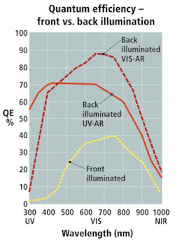
To increase the sensitivity of these devices, a process called backside thinning (BST) is used in which the backs of the imagers are thinned and combined with other techniques to extend the wavelength range of the imager from the visible to the UV. “There are,” says Joseph Sgro, CEO of FastVision (Nashua, NH, USA; www.fast-vision.com), “three main BST schools of thought. While companies such as Sarnoff (Princeton, NJ, USA; www.sarnoff.com) use BST and laser annealing, the BST process adopted by Fairchild Imaging (Milpitas, CA, USA; www.fairchildimaging.com) is performed using a selective chemical etching.
An alternative approach from the Jet Propulsion Laboratory (JPL; Pasadena, CA, USA; www.jpl.nasa.gov) uses BST and a layer of boron-doped silicon on the back surface.” Results of Sarnoff’s BST method, for example, show a substantial improvement in sensitivity especially in the UV region (see Fig. 1).
While improvements in BST techniques are increasing the sensitivity of these devices, other manufacturers are increasing the speed and reducing the noise of their CMOS imagers and cameras to take advantage of the vastly improved sensitivity promised by the use of UV illumination. To differentiate their product offerings, camera vendors are realizing that they too must become involved in developing the next generation of these sensors.
For example both Basler Vision Technologies (Ahrensburg, Germany; www.baslerweb.com) and Dalsa (Waterloo, ON, Canada; www.dalsa.com) have introduced CMOS cameras based on their own designs, and it is certain that this trend will continue. While such developments will be especially beneficial to the semiconductor industry, camera vendors must also develop faster-than-Camera-Link interfaces with which to transfer data from their cameras.
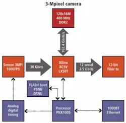
“Likely as not,” says Sgro, “these interfaces will be based on parallel fiberoptic links that increase data transfer speeds to more than 30 Gbits/s.” Indeed, in its next-generation camera design, FastVision will use a 3-Mpixel imager from Cypress Semiconductor (San Jose, CA, USA; www.cypress.com) coupled via a Xilinx gate array to a 12 × 2.7-Gbit/s parallel fiberoptic link from Zarlink Semiconductor (www.zarlink.com; see Fig. 2). By using 12 parallel channels, each with a data rate of 2.72 Gbits/s/channel, a total 32.6-Gbit/s data rate is achievable, more than five times faster than the maximum achievable Camera Link data rate. To provide analog and digital timing, automatic pixel signal nonuniformity correction, dark signal nonuniformity calibration, and automatic camera control, the camera will also incorporate a PNX1500 TriMedia processor from NXP (Eindhoven, The Netherlands; www.nxp.com).
High-speed cameras that use such fiberoptic links will also mandate the development of host frame grabbers to transfer these images from the camera to the host PC. Luckily the PCI Express standard can support bidirectional data rates of 8 Gbytes/s when x16 lane boards are used. To date, however, these boards have been limited to graphics products, where balanced I/O is not a necessity.
However, this may change with the more balanced I/O instruction and data approach taken in the PCI Express Version 2 standard (see “Fast and Faster,” pp. 33–37). “However, in the semiconductor industry,” says Sgro, “the task of processing such large amounts of data is often not performed by off-the-shelf frame grabbers and image processors. Rather it is relegated to in-house-developed frame grabbers and image processors that are programmed to perform specific tasks.


