December 2017 snapshots: Google Clips camera, embedded vision in GenICam, self-learning chip from Intel, observing the solar eclipse with an infrared camera.
Researchers use infrared camera to observe solar eclipse
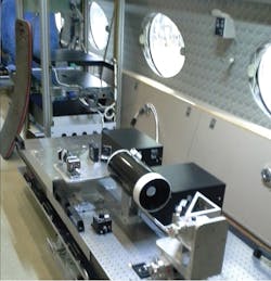
Aided by funding from a National Science Foundation Major Research Instrumentation grant, researchers deployed the Airborne Infrared Spectrometer (“AIR-Spec”), which featured an infrared camera for observation and measurements during the 2017 “Great American Solar Eclipse.”
AIR-Spec inside the Gulfstream V, credit Harvard Smithsonian Center for Astrophysics
The members of the research team included the Smithsonian Astrophysical Observatory (Cambridge, MA, USA; www.cfa.harvard.edu/sao), Harvard University (Cambridge, MA, USA; www.harvard.edu), the National Center for Atmospheric Research Aviation Facility and the High Altitude Observatory (NCAR; Boulder, CO, USA; https://ncar.ucar.edu/). The team’s AIR-Spec instrument was used to measure five magnetically-sensitive coronal emission lines during the eclipse from the NSF/NCAR Gulfstream-V High-performance Instrumented Airborne Platform for Environmental Research (GV HIAPER).
AIR-Spec’s optical design elements included an f/15 Cassegrain telescope, 100 g/m grating with 9.8° incidence, a 75 µm slit, a camera fold mirror, a spherical 0.7 m focal length collimator, spherical 0.5 m focal length focus mirrors, and an infrared camera. The team used an IRC912 MWIR camera from IR Cameras (Santa Barbara, CA, USA; www.ircameras.com), which features a 1280 x 1024 Indium Antimonide (InSb) MWIR detector. The detector has a spectral response of 1 to 5.3 µm and a pixel pitch of 12 µm and can reach a frame rate of 119 Hz.
Aboard the GV HIAPER, the AIR-Spec instrument was flown along the path of totality of the solar eclipse and was used to make measurements of the solar corona in the infrared spectrum, thereby increasing the understanding of various phenomena including solar wind and plasma heating and acceleration, according to IRCameras.
Google Clips camera uses machine learning to capture spontaneous moments in everyday life
Google (Mountain View, CA, USA; www.google.com) has announced the release of Google Clips, a small, hands-free camera that uses a machine learning algorithm to look for good moments to capture in everyday life.
An image sensor size or model is not named—though The Verge (New York, NY, USA; www.theverge.com) is reporting that a 12 MPixel sensor is being used—but the camera features a 1.55 µm pixel size, auto focus adjustment, a 130° field of view, a frame rate of 15 fps, auto low lux and night mode, 16 GB storage, as well as motion photos (JPEGS with embedded MP4s), MP4, GIF, and JPEG, with no audio. Additionally, the camera has Gorilla Glass 3 for durability, as well as USB-C, Wi-Fi Direct, and Bluetooth LE for connectivity.
Running on Android, Clips also features Moment IQ, a machine learning algorithm that Google says is smart enough to recognize great expressions, lighting, and framing, while always learning. As more images are captured with Clips, the camera will learn to recognize the faces of people that matter to you and will help capture more moments with them, according to Juston Payne, Google Clips Product Manager.
Google Clips’ algorithm runs in real time directly on the camera with the Movidius Myriad 2 vision processing unit (VPU), which the company calls the industry’s first “always-on” vision processor. This VPU contains hybrid processing elements including 12 128-bit VLIW processors called SHAVEs, and an intelligent memory fabric that pulls together the processing resources to enable power-efficient processing. It also has two CPUs and a software development kit to incorporate proprietary functions.
“To bring our vision for Clips to life, we’ve been working on integrating Intel’s Movidius technology within Clips to give people many of the benefits of machine learning directly on their device,” said Google Clips product lead Juston Payne. “On-device processing gives people a lengthy battery life, speedy access to their clips, and the ability to use the camera without an internet connection. We can’t wait for parents and pet lovers to start effortlessly capturing spontaneous moments, while getting to stay in the moment.”
Remi El-Ouazzane, vice president and general manager of Movidius (San Mateo, CA, USA; www.movidius.com) Intel (Santa Clara, CA, USA; www.intel.com) New Technology Group, also commented: “In our collaboration with the Clips team, it has been remarkable to see how much intelligence Google has been able to put right into a small device like Clips,” he said. “This intelligent camera truly represents the level of onboard intelligence we dreamed of when developing our Myriad VPU technology.”
Clips taken from the camera sync wirelessly and, in seconds, from the camera to the Google Clips app for Android or iOS. Privacy issues are addressed in the blog post written by Payne. In it, he explains that the camera lights up so people will know when it is on and capturing, to make it clear to people when is being used.
Google Clips will be available soon in the U.S. for $249, with the first edition being designed specifically with parents and pet owners in mind.
Progress update on integrating embedded vision into GenICam
Embedded image processing devices have until recently consisted of cameras or vision sensors interfaced to heterogeneous processing units such as CPUs, GPUs, FPGAs and SoCs (System on Chip), a combination of processors or processing modules. The focus of the IVSM (International Vision Standards Meeting) standardization body is the software-side harmonization of these various elements during its semi-annual sessions and progressively moving solutions forward. To achieve standardized data exchanges within image processing devices, the panel plans to further develop the GenICam camera standard, which will ensure the rapid implementation and cost-effective operation of devices.
At the October 2016 meeting in Brussels, the IVSM panel agreed to tackle the two most important standardization aspects of connecting subcomponent software: The description of pre-processing and its results using so-called processing modules, and secondly connecting various XML data which serve the cameras’ standardized parameter and function descriptions.
The results of these discussions were presented at the following meeting in Boston in May 2017 where further implementation was specified. One challenge in standardization is posed by changing image data formats, as well as by the input and output formats of processing modules that the application software accesses and then must dynamically interpret. Additionally, an interface structure is needed that will link data from camera sensors and processors with those of the processing modules.
In the future, different image and pixel formats as processing module output data — such as raw, binary, RGB or blob images — with additional metadata such as enlarged or reduced images and/or image details (ROI) would be uniformly described using XML and integrated into the new general streaming protocol GenSP (GenICam Streaming Protocol). This would allow the standardization of a process such as turning processing on and off in order to retain or change the input image data. As an example, in the case of a laser profiling image, the laser line can be dynamically switched on or off. Another example would be the parameter description of the image formats should be valid for all camera interfaces.
Uniform XML Descriptions
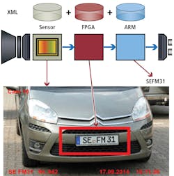
Just as image formats must be flexibly described, so must those of the processing modules, as well as camera sensors and processors, for a proper interconnection to occur. The application software will then be able to read the camera’s parameters in a standardized and automated fashion, and to determine which data the camera delivers with which parametrization. In this method common changes made by various manufacturers can be uniformly implemented such as the camera parameters’ XML and that of its preprocessing would be merged.
Flexible modules that can represent one unit as a processing module in relation to the preprocessing (consistent with GenICam SFNC), could replace highly optimized individual components. Parameter trees of both the processing module and the camera are then merged into a single tree. In the future, the tool that merges the trees will be made available in the GenICam Repository, ensuring uniform readability of all cameras within sensor groups.
In the embedded world, the use of FPGAs is pervasive and is also described by the GenICam standard. ARM processors are too slow for the image processing tasks required and are instead better suited for post-processing. By contrast, FPGAs meet the demands on computational performance and for heat build-up, are extremely well suited for preprocessing, and are built into practically all cameras. Combinations of FPGAs with GPUs and CPUs are possible. With the embedded GenICam standard that is being created, these processor modules will coalesce into one homogenous unit with a consistent data structure.
Summary: In implementing a new embedded vision standard for the software level, the IVSM Committee is placing particular emphasis on XML-based descriptions. XMLs are widely used in the GenICam GenAPI standard, and they define semantics and their interpretation for camera descriptions. Equally well known in GenICam are the processing modules that were first used for 3D line scan camera description. Further steps in implementing the standard will be covered in future briefings.
This article was written by Martin Cassel, Silicon Software (Mannheim, Germany; www.silicon.software)
Self-learning chip from Intel aims to speed artificial intelligence by working like the human brain
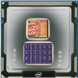
Codenamed Loihi, Intel’s (Santa Clara, CA, USA; www.intel.com) new self-learning neuromorphic chip is reportedly able to mimic how the human brain functions by learning to operate based on various modes of feedback from the environment, with an ultimate goal of speeding artificial intelligence technologies, according to the company.
Billed as a “first-of-its-kind” chip from the company, Loihi uses data to learn and make inferences and uses an asynchronous spiking computing method, which enables it to use data to learn and make inferences, and get smart over time, much like the brain, according to Intel.
“We believe AI is in its infancy and more architectures and methods – like Loihi – will continue emerging that raise the bar for AI,” according to Dr. Michael Mayberry, corporate vice president and managing director of Intel Labs. “Neuromorphic computing draws inspiration from our current understanding of the brain’s architecture and its associated computations.”
He added “The brain’s neural networks relay information with pulses or spikes, modulate the synaptic strengths or weight of the interconnections based on timing of these spikes, and store these changes locally at the interconnections. Intelligent behaviors emerge from the cooperative and competitive interactions between multiple regions within the brain’s neural networks and its environment.”
Loihi’s test chip, which in 2018 will be shared with leading university and research institutions with a focus on advancing artificial intelligence, includes digital circuits that mimic the brain’s basic mechanics, making machine learning faster and more efficient while requiring lower compute power. The neuromorphic chip models draw inspiration from how neurons communicate and learn, using spikes and plastic synapses that can be modulated based on timing, which could help computers self-organize and make decisions based on patterns and associations, according to Intel.
The test chip offers on-chip learning and combines training and inference on a single chip, which allows machines to be autonomous and to adapt in real-time.
“The self-learning capabilities prototyped by this test chip have enormous potential to improve automotive and industrial applications as well as personal robotics – any application that would benefit from autonomous operation and continuous learning in an unstructured environment. For example, recognizing the movement of a car or bike,” suggested Mayberry.
Features of the test chip, as described in an Intel press release, will include:
- Fully asynchronous neuromorphic many core mesh that supports a wide range of sparse, hierarchical and recurrent neural network topologies with each neuron capable of communicating with thousands of otherneurons.
- Each neuromorphic core includes a learning engine that can be programmed to adapt network parameters during operation, supporting supervised, unsupervised, reinforcement and other learningparadigms.
- Fabrication on Intel’s 14 nm process technology.
- A total of 130,000 neurons and 130 millionsynapses.
- Development and testing of several algorithms with high algorithmic efficiency for problems including path planning, constraint satisfaction, sparse coding, dictionary learning, and dynamic pattern learning andadaptation.
“As AI workloads grow more diverse and complex, they will test the limits of today’s dominant compute architectures and precipitate new disruptive approaches,” said Mayberry. “Looking to the future, Intel believes that neuromorphic computing offers a way to provide exascale performance in a construct inspired by how the brain works.”
He added, “I hope you will follow the exciting milestones coming from Intel Labs in the next few months as we bring concepts like neuromorphic computing to the mainstream in order to support the world’s economy for the next 50 years. In a future with neuromorphic computing, all of what you can imagine – and more – moves from possibility to reality, as the flow of intelligence and decision-making becomes more fluid and accelerated.”
Announcing the Loihi chip is just the latest headline regarding artificial intelligence and cutting edge vision-related technologies to come from Intel. Recent, relevant news includes the launch of the Movidius Myriad X vision processing unit (VPU), which is a system-on-chip that features a neural compute engine for accelerating deep learning inferences at the edge.
The neural compute engine is an on-chip hardware block specifically designed to run deep neural networks at high speed and low power without compromising accuracy, enabling devices to see, understand and respond to their environments in real time, according to Intel, which says that the Myriad X architecture is capable of 1 TOPS (trillion operations per second) of compute performance on deep neural network inferences.


