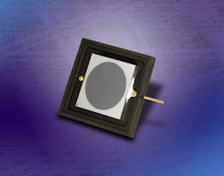
Opto Diode’s AXUV63HS1 - High-Speed, 9 mm² Circular Photodiode for Electron Detection
Opto Diode Corporation, an ITW company, announces a new high-speed photodetector, the AXUV63HS1. With a circular active area of 9 mm diameter (typically 63 mm²), the photodiode is ideal for electron detection. The new device joins Opto Diode’s family of AXUV detectors that features high-performance measurement of electrons, photons, or X-rays.
The AXUV63HS1 has a typical rise time of 10 nsec and a maximum dark current of 100 nA, with a minimum reverse breakdown voltage of 160 Volts. To view other specifications and responsivity graphs, please download Opto Diode’s data sheet here: https://optodiode.com/pdf/AXUV63HS1DS.pdf.
Opto Diode’s high-speed photodiode is shipped with a cover plate to protect the photodiode chip and the wire bonds. Storage and operating temperatures range from -10 °C to +40 °C (ambient) and from -20 °C to +80 °C in nitrogen or vacuum environments. The lead soldering temperature is 260 °C.
To learn more about Opto Diode’s AXUV family of detectors that detects energy from 100eV to 50keV for the measurement of electrons, photons, and/or X-rays from 0.0124 nm to 190 nm, please contact [email protected] or visit: https://optodiode.com/photodiodes-axuv-detectors.html.
Opto Diode Corporation (Camarillo, CA - www.optodiode.com), an ITW Company, delivers industry-leading sensors, photodiodes, IR detectors, photonic modules, assemblies, and LEDs. Available in standard and custom designs, Opto Diode products have earned a reputation for high performance, superior quality and reliability for over 30 years. Opto Diode offers advanced performance sensors from the extreme ultraviolet (UV) to the mid-infrared (mid-IR). Our products provide unparalleled high-energy particle, electron, X-ray, and UV detection along with superior sensitivity to discriminate trace gases or detect heat, sparks, or flames in the mid-IR spectrum. Other products include high performance LEDs with radiometric emissions from 365 to 940 nm and IR emitters covering 1 to 10 microns.
Opto Diode serves a variety of industries including aerospace, automotive, biotechnology, food processing, medical, military/defense, industrial, semiconductor equipment manufacturing, and test & measurement. Our manufacturing process is in a cleanroom environment, from start to finish. Opto Diode’s domestic U.S. facility is optimized for design and manufacturing with an on-site wafer fabrication, class 1,000 to class 10,000 clean rooms, extensive assembly capabilities and packaging expertise. From prototyping to high-volume production, we manufacture wafers-to-components then package and assemble photonic modules-to-optoelectronic sub-systems. For more information, visit www.optodiode.com.
