Low-cost development tools reduce the cost of embedded vision
FPGAs, reconfigurable processors, systems-on-a-chip (SOC) and off-the shelf development software are speeding the time to market of embedded vision systems.
In a recent article published in EETimes Europe, Nitin Dahad reported that Yole Développement (Lyon-Villeurbanne, France; www.yole.fr) has predicted a 140% growth in embedded vision over the next four years (see “Embedded Vision, Edge AI Drive Smart Industry,” February 2019; http://bit.ly/VSD-EET). Whether such a figure is achievable remains to be seen.
Certainly, however, the growth in embedded vision systems has been impressive over the past five years with numerous companies offering intellectual property (IP) for field-programmable gate arrays (FPGA), programmable “vision processors,” for both off-the-shelf and system-on a chip (SoC) development, and a host of software ranging from primitive pixel-based algorithms for such functions as bad pixel correction to filtering and color correction through sophisticated Simultaneous Localization and Mapping (SLAM) tools for robotic applications. To ease product development, many vendors now provide both public domain and proprietary application programming interfaces (API) with which to configure embedded hardware.
Video manipulation
When FPGAs began to be used in image processing applications, much of the IP was based on the distribution, compression, and broadcasting of video. By embedding functions such as H.264 and JPEG encoding and decoding, and video interlacing and de-interlacing into FPGAs, broadcast engineers could pipeline these functions resulting in faster, lower-cost equipment.
Today, such functions remain available from both FPGA vendors and their alliance partners. As part of the Xilinx (San Jose, CA, USA; www.xilinx.com) Alliance program, for example, VYUsyn (Bengaluru, Karnataka, India; www.vyusync.com) offers its H.264 1080p60, 4:2:2, a 10-bit decoder core which the company claims has been shipped in over 100,000 broadcast-related products.
Similarly, intoPIX (Mont-Saint-Guibert, Belgium; www.intopix.com), an Altera (Intel; Santa Clara, CA, USA; www.intel.com) Design Solutions Network Member, offers its Emmy Award-winning JPEG 2000 Encoder and Decoder IP-Cores that can be used in digital cinema, medical imaging, and remote sensing applications.
While initially targeted at broadcast engineers, the IP offered by FPGA vendors and their partners eventually expanded to encompass low-level, per-pixel based image-processing functions. Since functions such as histogram equalization, bad pixel correction, image filtering, Bayer interpolation, and color matrix conversion (from, for example, RGB to YIQ) operate on single pixels or groups of pixels in an image, they can be easily pipelined.
At present, for example, bad pixel correction in images is performed using an adaptive median filter. Here, an image’s bad pixels are identified as image noise and replaced by a filtered value. Then, a convolution matrix is passed over the image to obtain the filtered pixel value. Since image filtering, Bayer conversion, and color matrix conversion use similar techniques, these functions can be easily implemented as IP in an FPGA.
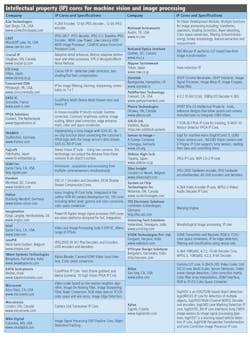
Today, numerous companies offer such IP to developers of machine vision and image processing systems (Table 1). These include IP for defective pixel correction from CIS Corp (Tokyo, Japan; www.ciscorp.co.jp), image convolution (filtering) cores from Concurrent EDA (Pittsburgh, PA, USA; www.concurrenteda.com), and color space conversion from iWave Systems (Bengaluru, Karnataka, India; www.iwavesystems.com.)Niche needs
While such algorithms are now common building blocks offered by IP vendors, some companies offer niche image processing IP for specific market needs. These include such functions as haze reduction, morphology, and video tracking. (http://bit.ly/VSD-NSW.)
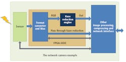
Nippon Systemware (NSW; Tokyo, Japan; www.nsw.co.jp/english) offers an IP core for haze reduction that can be used with Altera and Xilinx (San Jose, CA, USA; www.xilinx.com) devices. The “Haze Reduction Engine” reduces haze or fog in RGB images and targets such applications as networked surveillance cameras and smart vehicles (Figure 1).
Mathematical morphology, a technique pioneered by Jean Serra and Georges Matheron at the Centre of Mathematical Morphology (CMM) of the École des Mines de Paris in 1964, is often used to process and analyze the structure of objects within images.
Using the morphological operators of erosion, dilation, and opening and closing, specific shapes can be determined. Since the structuring elements are moved over the image, the technique is well suited to implementation within FPGAs. This is the aim of the Morphological Image processing IP core from Unistring Tech Solutions (Hyderabad, Telangana, India; www.unistring.com) that is designed to perform erosion, dilation, opening and closing functions on Xilinx Spartan and Vertex FPGAs (http://bit.ly/VSD-UTS).
Other specialized functions such as video tracking are also being offered by IP vendors. One such example, the FPGA IP core T-COR-32 from SOLID Ltd. (Vladimir, Russia; www.solidtech.systems) tracks objects in video and calculates their motion parameters. In the case of object loss (tracking collapse), the IP core predicts the tracked object trajectory until it is retracked. As a standalone IP core, T-COR-32 is compatible with Altera and Xilinx FPGAs (http://bit.ly/VSD-VTF).Camera connections
Just as pixel-based functions can be implemented in FPGAs, so too can the protocols required to interface them to standard camera interfaces. In this way, both the camera interface and image pre-processing functions can be embedded into single FPGA devices.
Several vendors offer IP for implementing camera interfaces such as USB, Camera Link and CoaXPress (CXP) in FPGAs. Sensor to Image (now owned by Euresys; Schongau, Germany; www.s2i.org), for example, offers a set of IP cores and a development framework that provide a set of registers required for a USB3 Vision camera. Additionally, conversion of image data streams from an image sensor to the format required by the USB3 PHY (http://bit.ly/VSD-PHYC ) can be achieved.
Similarly, Microtronix’s (London, ON, Canada; www.microtronix.com Camera Link Transceiver IP Core can be used to implement the standard’s Base, Medium and Full configurations. Supporting camera control signals, serial communication, and video data, the IP core supports clock rates of up to 85 MHz.
For those wishing to implement high-speed camera interface standards such as the CXP standard, the CoaXPress IP Core from KAYA Instruments (Nesher, Israel; www.kayainstruments.com) provides both host and device modes of operation and can be implemented using a number of different FPGAs including Xilinx Virtex and Intel (Altera) Cyclone devices.
While some manufacturers provide IP cores to perform image processing and camera interface functions, others also provide much of the IP required to interface FPGAs to external camera systems and computer interfaces.
iWave Systems, for example, offers a number of interface cores that include PCI controllers, PCIe to UART, and PCIe to SD-MMC bridges. Many of these companies are listed on the websites of both Intel and Xilinx.
Point (e.g. per pixel) and local transforms (e.g. convolution) form the basis of many image processing functions and are well suited to being implemented as pipelined functions in FPGAs. Global transforms such as the Fourier transform that produce an output pixel value at every pixel based on multiple values in the input image are also suited for such embedded approaches.
To do so, developers could opt for application specific ICs to perform this task. Indeed, in 2002, there were no less than five companies that manufactured ASIC devices that performed this task (see “FFT benchmarks position ASICs for imaging applications”; Vision Systems Design, November 2002; http://bit.ly/VSD-FFT).
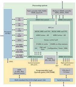
Today, such global transforms can be performed with fast general-purpose processor/FPGA combinations, graphics processors or vision processor ICs that are offered as IP. For example, Xilinx’s LogiCORE IP Fast Fourier Transform (FFT) core implements the Cooley-Tukey FFT algorithm, a computationally efficient method for calculating the Discrete Fourier Transform (DFT). Because the IP can be implemented on devices such as the Xilinx Zynq-7000 (Figure 2), other image processing algorithms can be added since dual-core ARM Cortex-A9 processors integrated with Artix-7 or Kintex-7 programmable logic and transceivers running from 6.25Gb/s to 12.5Gb/s are available on-chip. Examples of how the device can be used in machine vision and image processing applications can be found here: http://bit.ly/VSD-REV.Core technology
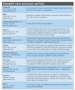
While vendors such as Xilinx provide processor/FPGA combinations, others such as Synopsys (Mountain View, CA, USA; www.synopsys.com) offer processor cores optimized for embedded vision applications. The company’s DesignWare EV61, EV62 and EV64 embedded vision processor cores integrate one, two, or four vision CPU cores and a programmable convolution neural network (CNN) engine.
The CNN engine operates in parallel with the vision CPUs for object detection and image classification. The EV6x processor family is supported by a programming environment based on embedded vision standards including OpenVX. OpenCL and Synopsys’ MetaWare Development Toolkit.
One of the first companies to integrate the ev62 core is Inuitive (Ra’anana, Israel; www.inuitive-tech.com). Using the core, the company has developed its NU4000 3D imaging and vision system on-chip (SoC). Using the MetaWare EVdevelopment toolkit, computation between the vision CPU and CNN resources can be distributed to support neural network algorithms and customer-specific CNN layers.
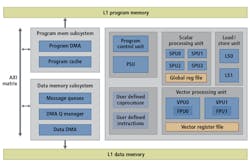
Like Synopsys, CEVA (Mountain View, CA, USA; www.ceva-dsp.com) licenses signal and image processing IP and AI processors to manufacturers for embedding into their own custom ICs. Although the architecture of its CEVA-XM4 imaging and computer vision processor IP is dissimilar to that of Synopsys’ EV6x processor family, programming the fully synthesizable DSP and memory subsystem IP core can be accomplished in high-level languages (Figure 3).Recently, the IP core was adopted by NextChip (Seoul, South Korea; www.nextchip.com) in its APACHE4 vision-based pre-processor SoC. Using a dedicated sub-system incorporating CEVA’s programmable vision IP and an array of dedicated processors for pedestrian, vehicle, and lane detection, and moving object detection, the device will be targeted toward next-generation advanced driver-assistance systems.
Camera development
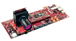
To aid developers in integrating these processor/FPGA combinations into machine vision products, companies such as Avnet Silica (Brussels, Belgium; www.avnet.com) offer embedded camera development kits. These include the Picozed embedded vision kit (Figure 4) based on the Xilinx Zynq-7000 SoC and the Avnet Silica STM32F7, a development kit that is based on NXP’s (Eindhoven, Netherlands; www.nxp.com) Kinetis K82F Cortex-M4 microcontroller. With a USB interface, a 4.3-inch color capacitive touchscreen display, and a miniature VGA (640 x 480) camera module, the kit is able to capture still images or stream real-time low-resolution video.Other embedded imaging systems vendors are also offering starter kits based on industrial cameras from well-known machine vision vendors. AAEON Europe (Langen, Germany; www.aaeon.com), for example, has developed the UP Embedded Vision Starter Kit that includes an x86 processor board with both USB 3.0 and GigE interface support and the Dart 5 MPixel board-level industrial camera from Basler (Ahrensburg, Germany; www.baslerweb.com).
Rather than take this approach, Allied Vision (Stadtroda, Germany; www.alliedvision.com) has chosen to develop an application-specific integrated circuit (ASIC) to power its Alvium embedded vision camera modules. The ASIC used is, in essence, an image signal processor that can be programmed with Allied Vision’s Image Processing Library.
Although the architectures of FPGAs, FPGA/processor combinations, and custom machine vision devices are complex, manufacturers have recognized the need to offer high-level development tools with which to program them. To speed the development of such embedded vision systems, many manufacturers now support OpenCV (opencv.org), an open-source computer vision library. Xilinx, for example, has produced a device optimized for OpenCV FPGA library, the Xilinx OpenCVlibrary, that is intended for application developers using Zynq-7000 SoC and Zynq UltraScale+ MPSoC devices (http://bit.ly/VSD-XOC).
About the Author

Andy Wilson
Founding Editor
Founding editor of Vision Systems Design. Industry authority and author of thousands of technical articles on image processing, machine vision, and computer science.
B.Sc., Warwick University
Tel: 603-891-9115
Fax: 603-891-9297
