MWIR imaging maintains the quality of laser welds
Using an MWIR imager, a monitoring and control system captures images of laser welding at high speed.
Rodrigo Linares
Due to their inherent efficiency, repeatability and ease of maintenance, the use of lasers in automobile manufacturing has increased dramatically over the last decade. While most laser-based systems are predominantly used to cut parts, a significant number are employed in other applications such as welding, marking and additive manufacturing.
During the laser welding process, changes in process parameters can affect the quality, size and properties of a welded joint. Any such changes that do occur may compromise the mechanical behavior of the welded component, leading to a failure in service. Hence, monitoring and controlling the laser welding process has become vitally important to ensure the quality of welded joints.
To perform this task, researchers at three European companies and institutions are working to create a laser welding monitoring and control system. Under the auspices of an EU-funded project called Laser equipment ASessment for High impact innovation in the manufactuRing European industry (LASHARE), New Infrared Technologies (NIT; Boadilla del Monte, Spain; www.niteurope.com) AIMEN Centro Tecnológico (Porriño, Spain; www.aimen.es) and Centro Ricerche Fiat (Orbassano, Italy; www.crf.it/en-US/Pages/default.aspx) have joined forces to develop a system that can ascertain the quality of welded sheets of steel by capturing and processing images of the welding process from an uncooled MWIR sensor.
Laser welding
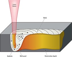
Laser welding is predominantly used in applications in the automotive industry because it enables very deep and narrow welds to be created. In a laser welding system, the power of the laser melts and partly vaporizes metal, creating a cavity called the "keyhole" (Figure 1).
To ensure the quality of welds achieved by the laser welding process, the thermal distribution and the geometric size of the keyhole and the weld pool that is created around it can be monitored and controlled by measuring and characterizing the various forms of electromagnetic radiation that propagate from them.
There are a variety of such emissions that can be measured. Electromagnetic radiation in the infrared (IR) region, for example, is generated by the molten material in the weld pool, while visible and UV radiation is emitted by the plasma above it. Airborne acoustic waves are also generated by the displacement of air due to evaporation, heating and expansion of the material.
Currently, most weld monitoring systems detect at least one of these parameters. Potentially, the use of a high-speed IR area imager would offer several important advantages over these traditional measurement techniques. However, in the past, the high complexity and cost associated with devices such as quantum IR detectors has previously precluded their use. While lower-cost alternatives such as microbolometers or pyroelectric devices are available, they have a fundamental limitation due to their slow response time.
Recently, however, an IR imager called Tachyon has been developed at NIT that allows the spatial distribution of the heat around the weld to be measured and how this distribution changes during the welding process. In addition, the device can acquire image data at a fast enough rate to ensure that it can capture images of any defect that may be present.
The Tachyon device-which was used in the system developed by the EU consortium partners-is a quantum IR imager that has been monolithically integrated with Si-CMOS readout circuitry. In the welding monitoring system, the sensor was used to capture low resolution, 32 x 32 pixel images at frame rates up to 10kHz in uncooled operation, at a cost comparable with traditional IR spot detectors.
The high sampling frequency of the NIT imager is significant because it enables the device to capture images at least twice as fast as the frequency of the welding phenomena that cause welding defects, which can occur at rates up to 5kHz. So too is the fact that it can capture images-unlike most infrared spot detectors which cannot provide relevant information about the temperature distribution over an area, or data relating to the dynamics of the heat transfer process.
Imaging in action
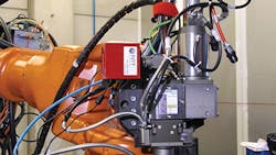
In an experiment to determine the potential of the IR imager in a laser welding application, an imager in a standard CMOS camera was replaced with the NIT device. No specific optical arrangement was fitted to the camera; the broadband imager was deployed in the camera without a lens to capture light that spans the short and mid-IR wavelengths between 1-5µm. To image the welding process, the camera was fixed onto a WT03 laser welding head from Permanova Lasersystem's (Mölndal, Sweden; www.permanova.com) fitted with a 4.4 kW Nd:YAG laser from Rofin Sinar (Hamburg, Germany; www.rofin.com) with a power range between 2700-4000W.
The camera was mounted in a coaxial arrangement with the laser onto an IRB 6600 robot from ABB (Zurich, Switzerland; www.abb.com) so that it could directly capture images of the melt pool during the welding process. The six-axis IRB 6600 robot moved the laser at speeds of 20-45mm/s to lap weld together two different zinc-coated steel sheets, while the camera captured images of the process. During the welding procedure, the data captured by the imager was transferred to a PC based system over a USB 2.0 interface where a real time analysis of the images and defect classification was performed (Figure 2).
To provide a visual indication of the thermal distribution across the welding surface, custom software written in Matlab takes the images captured by the camera and identifies the brightest point in the image. Having done so, a rectangular 1 x 32 pixel slice of each 32 x 32 image is created with the brightest point in the image. These image slices are then stitched together in software to form a continuous rectangular image that provides a visual indication of the heat distribution across the welded joint as it occurred in real time.
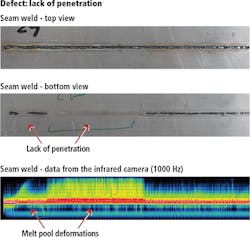
Using this technique, images from the sensor were used to identify a lack of fusion between the two welded sheets. Figure 3 shows a visible image of the top and the bottom of a joint taken after one pass of the laser welding head. From the image of the top of the material, it would appear that the welding process has been successful. However, the visible image of the bottom surface of the joint highlights the fact that the laser has not fully penetrated the material. The images captured from the top surface of the joint with the IR camera show that the cause of the defect is due to the deformation of the weld melt pool which has led to an uneven distribution of the heat across the top surface of the joint.
Machine learning
While such visual indications of the thermal distribution across the weld are useful, the ultimate goal of the research project was to enable the PC-based system to analyze the data captured by the camera to enable faults to be automatically identified and classified. To do so, a machine-learning system was developed which enabled four common types of welding defects to be classified. These defects are caused by a lack of penetration due to an excessive gap between the sheets of metal, deformation of the sheets themselves, a lack of weld and open pores.
To train and test the machine-learning system, a data set of images of both good and defective joints was created from the images acquired during the welding process. The images were then labeled as to whether they represented a good or a defective joint. The images of the defective joints were then further labeled according to the type of defect they represented.
Due to the fact that a large quantity of data is created during the image acquisition process, the size of the data set was reduced to enable the system to perform defect detection and classification. To do so, a Principal Component Analysis (PCA) technique was employed which reduced the high-dimensional space of each set of images into a set of lower dimensional subspaces. Finally, the lower dimensional sets of PCA data were used to train a support vector machine (SVM) to analyze the data set and to recognize patterns in it that represent the four different types of welding faults.
Once the machine learning system had been developed, an analysis was performed to examine how effective it was at identifying the four classes of defects. To do so, raw image data from the sensor were transferred to the PC during a welding operation. The software on the PC then applied the PCA reduction technique to the data set and generated a new array of values. A k-Nearest Neighbors algorithm (kNN) then first classified the values as either representative of a good weld or a faulty weld, after which the faulty welds were further classified into the type of defect by the SVM.
Having conducted a number of such welding operations, it was possible to analyze how effective the machine learning system was at classifying the types of defects. The results of the analysis showed the number of defects detected as well as the true positives (TP), the false positives (FP) and the false negatives (FN). From these results, a confusion matrix was built to enable the performance of the machine learning algorithm to be revealed (Table 1).
Even though the sensor was set up in a standard laser head without any type of modification, most of the weld defects were detected with a success rate as high as 98.8%, and only 10.4% of the defects were not properly identified. It was clear from the results however, that the system was more effective at classifying gaps between the metal sheets and open pores than it was at detecting deformation and lack of welds.
Further research is currently underway to determine if the machine learning system can be optimized further to improve its defect classification performance. Future improvements will also allow defects to be detected and classified at a faster rate. Ultimately, the aim is to develop a system that can identify the defects and use the data to control the welding process parameters to ensure the quality of the weld.
Rodrigo Linares,
Business Development Manager,
New Infrared Technologies,
Boadilla del Monte, Spain
Companies mentioned
ABB
Zurich, Switzerland
www.abb.com
AIMEN Centro Tecnológico
Porriño, Spain
www.aimen.es
Centro Ricerche Fiat
Orbassano, Italy
www.crf.it/en-US/Pages/default.aspx
New Infrared Technologies
Boadilla del Monte, Spain
www.niteurope.com
Permanova Lasersystem
Mölndal, Sweden
www.permanova.com
Rofin Sinar
Hamburg, Germany
www.rofin.com


