Low Power Image Sensors for Modern Vision Systems
Driven by faster connectivity speeds and increased automation and smarter systems, Industry 4.0 accelerated the adoption of vision in manufacturing and introduced intelligence into what were previously simple data capture systems. Prior-generation vision systems captured the images, packed them for delivery and provided the image data for downstream processing by FPGAs, ASICs or costly system on a chip (SoC) devices. Today, Industry 5.0 is building on these technology advances by incorporating artificial intelligence (AI) and machine learning (ML) in the entire data path and enabling mass customization. Cameras have become smart with the ability to process image data at an application level and output just the metadata for decision-making.
A key development between these generations was the focus on what happens at the edge. Our world is predominantly analog in nature and many electronic and electro-mechanical (EEM) systems that help us in everyday life are driven by sensory inputs. Vision (light), temperature (heat), audio (sound), proximity and position, pressure (touch) electronic sensors at the edge of the system capture these physical inputs and translate them into processed data to add intelligence and enable easy decision-making.
Industry 4.0 introduced the need for these sensors to become intelligent and efficient. Many sensors have now evolved with enhanced versions that adopt the processes and standards necessary for industrial automation efforts.
This widescale adoption of sensors also comes at a time when there is a drive for lower power, battery-operated smart devices embedded everywhere. Power presents different challenges for vision systems, and how image sensors address them can be a differentiating factor for the vision system.
In this article, I will discuss the technical challenges to overcome as well as the techniques engineers can use to decrease a sensor’s power consumption without sacrificing image quality and, thus, enabling efficient vision systems.
Related: The Evolution of Industry: What's to Come for Industry 5.0
Image Sensors—The Input Mechanism to Vision Sensing
Vision sensing has become a prominent method of capturing data at the edge. This collected image data can be used to quickly and efficiently make decisions. For example, without a vision sensor, a scene’s objects need innumerable and specific sensors to convey what the scene is made up of. This translates into a lot of data and colossal processing and, maybe with a lot of luck, a true representation of the scene. On the other hand, an image conveys everything in the scene in one frame of data resulting in a highly efficient system.
This ease of data representation has enabled image sensors to evolve at an accelerated pace to support consumer mobility products like smartphones, with resolution capabilities of more than 100 MPixel, and supported by hardware and software to deliver both detailed still images and video streaming.
Unlike the broad goals of consumer products, vision systems addressing automotive, industrial, and commercial applications serve highly purpose-oriented objectives, many of which use the (sensor) outputs for machine-based decision-making and demand a fine balance between resolution, frame rate, and power consumed.
Related: Industrial Computing Advances Power Evolution in Robotics, AI, Machine Vision
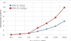
As the importance of intelligence at the edge begins to grow, these industrial applications must adapt to meet the needs of different use cases. Many are now demanding higher resolution and better overall performance to aid computer vision, machine vision, and automation decision systems. In many cases, greater detail is very much desired to provide the nuances needed to minimize erroneous decisions. As resolution increases, the number of pixels in an image sensor increases and correspondingly the image data delivered by the sensor to the image signal processor (ISP) or SoC. Huge image data from the sensor and the processing of the same by the ISP/SoC results in high power consumption, thereby placing an enormous burden on the vision system design. (See Figure 1)
So, how do designers of today’s vision systems and sensors solve these challenges?
It All Begins with Quantum Efficiency
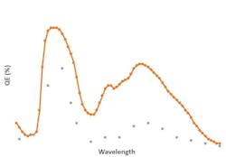
The quantum efficiency (QE) of an image sensor defines the ability of its photodiode to maximize the conversion of the incident photons into electrons. It is well known that the higher the QE, the better the image brightness. Higher QE is valuable in low light conditions and typically this is obtained by using a larger pixel size or by supplementing the scene with either visible or invisible illumination. In either case, there is added cost, added power and real estate that must be supported in the vision system, which could increase exponentially depending upon the image sensor capabilities and scene conditions. (See Figure 2)
This is particularly severe in the invisible illumination case that typically uses infrared light emitting diodes (IR LEDs), which generate light at 850 nm and 940 nm wavelengths sensed by image sensors but not by the human eye. In the industry, this is generally termed as “active illumination”. IR LEDs also consume power and thereby demand power delivery, significant real estate, and add substantial BOM (bill of materials) cost to the system. An image sensor having high QE in the NIR (near infrared) spectrum minimizes its quantity, intensity, and the overall BOM cost without compromising the image quality.
Related: 11 Myths About Image Sensors
Higher the Image Quality, Lower the Overall TCO
However, it’s important to ensure that the high QE delivered by the image sensor’s pixel is not impacted with noise in the rest of data path thus vitiating the overall image quality. For example, if the pixel architecture does not have sufficient pixel-pixel isolation, inter-pixel crosstalk could reduce the modular transfer function (MTF) and the contrast and sharpness of the image objects, ultimately affecting the image quality. Another impairment could be through poor readout circuitry resulting in high read noise.
Poor image quality places an undue burden on the ISP/SoC to do more, which either reduces the overall frame rate of the vision system or clock at a much higher rate to maintain the same end-end timing. In the former case, the vision system is substantially inefficient and, in either case, the system ends up consuming more power. To support the processing burden, an ISP/SoC with advanced resources might be needed, which increases the overall BOM cost.
Superior image quality output alleviates the shortcomings described above and reduces the overall TCO (total cost of ownership) of the vision system.
Subsampling Modes
Some image sensors (like the ones from onsemi Hyperlux LP product family) have recognized such operational needs and have incorporated a wide variety of subsampling modes. These modes like binning, cropping, and skipping reduce the bandwidth generated and transmitted substantially.
These capabilities make the vision system extremely smart, enabling it to choose the most optimal power/performance profiles needed based on the use-case needs. For example, in the case of a biometric scanner, a single system with a 5 MPixel sensor array can now be used in incremental severity of the scan process starting from a single fingerprint in a subsampled mode to a full resolution facial scan. Most importantly, the ISP/SoC receives less data to process, decreasing its power consumption and of the entire vision system.
Scale it Down
Larger resolution image sensors generate substantial bandwidth output. For example, a 20 MPixel sensor at 60 fps will transfer 12 Gbps of image data, which not only has to be handled carefully across the high-speed interfaces in the sensor but also by the ISP/SoC that receives them. Processing such large data requires expensive and dedicated resources within these processing engines and can result in substantial power consumption and thermal management issues. Furthermore, limitations on interfacing speeds add to this challenge.
In most applications, it’s likely that the full resolution in full operational speed is required only for a fraction of the operating time, with the rest of the duration being met with a lower resolution. While the subsampling modes can bring down the bandwidth and have their own merits, they are challenged with certain constraints in resolution selection or scene completeness.
Related: Bringing 20/20 Vision to the Edge with AI Inferencing
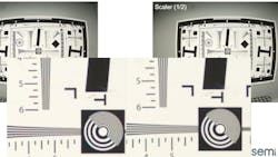
Scalers within the sensor come in handy to overcome these constraints and address the needs of lower resolution operation effectively. They provide the ability to control the bandwidth right at the source instead of being managed by the ISP/SoC. They can provide the freedom of granularity to the largest extent yet retain the complete FOV. Scaling algorithms can be highly sophisticated thus delivering substantially superior image quality even at significantly scaled resolutions. As an example, while 20 MPixel is certainly needed to acquire details of an object at distance, it may only be needed in a particular region of the image, not the entire image. By cropping or scaling to only this dynamically defined region you receive the benefit of a 20 MPixel sensor, without needing to consistently process 20 MPixel worth of data.
Sleep as Much as Possible, Wake Up on Demand
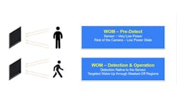
The sensor can be in a very low operational state—low resolution, lowest frame rate of operation for most of the operational time. It switches to a predetermined configuration when motion is detected—wake on motion (WOM). The image sensor has the native ability to resolve these changes and let the ISP/SoC switch it to the desired mode/configuration. It can further mask off regions where motion is not relevant to the application thus making the sensor and the vision system a lot more targeted and highly efficient. Previously, this function was done in the processor, but in doing so, the sensor reduces system resources and power.
We can see the profound impact of such capabilities in applications that are sourced through batteries, smart access systems, retail scanners, medical monitoring systems, and the like. Battery-powered applications derive the maximum benefit out of these sensors because they can minimize power consumed by the system. In a 4K video doorbell application, an 8 MPixel image sensor, which would transmit 6G data in its full operating state, can now be in the WOM mode more than 98% of operational time. During this pre-detect phase, it generates/transmits an extremely low amount of data and enables the entire vision system to operate at a fraction of the power consumed in full operating mode.
Image sensors have been doing an excellent job as data capture and data transfer devices. However, the above trends and advancements demonstrate how sensors need to become edge devices with application intelligence built into them. Through better pixel technology, configurable smart regions of interest, and integrations of functions like motion detection, they can now be designed to address specific use-case needs, resulting in differentiated and highly efficient vision systems that deliver superior performance while consuming very low power.
About the Author

Ganesh Narayanaswamy
Ganesh Narayanaswamy is responsible for management of the image sensors product line and business in the Industrial & Commercial Sensing Division (ICSD) at onsemi (Phoenix, AZ, USA). He focuses on bringing vision solutions to the commercial and industrial markets, and the business growth in multiple geographical regions. Narayanaswamy joined onsemi from Xilinx (San Jose, CA, USA) where he managed the industrial vision and electric drives businesses globally. Prior to that, he managed the Networking ASICs business at Avago (San Jose, CA, USA) and at ST Microelectronics (Geneva, Switzerland). Narayanaswamy also led the product marketing efforts for Structured ASICs at Altera (San Jose, CA, USA) and designed/developed multiple devices at National Semiconductor (Santa Clara, CA, USA). He holds an MBA from Santa Clara University (California) and a MS(EE) from Mississippi State University (Starkville).