Image Sensors: Novel sensor designs tackle multispectral applications
While the Bayer filter is perhaps the most well-known color filter array currently in use, a number of recent variations of both filter and photodiode structures have led to the development of image sensors targeted at consumer, security and x-ray applications (see "Image sensors build on the brilliance of Bayer," Vision Systems Design, March 2014). More recent developments presented at this year's Photonics West show in San Francisco, CA, showed how companies are tailoring such filter designs to meet the needs of cameras developed specifically to image polarized light and analyze multispectral images.
Two years ago, researchers at the Fraunhofer Institute for Integrated Circuits (Erlangen, Germany; www.iis.fraunhofer.de) developed a camera dubbed Polka that uses a custom sensor to replace the analyzer used in conventional polariscopes. To do so, a 560 x 256 pixel CMOS image sensor is overlaid with a 2 × 2 matrix of polarizing filters. (see "Smart camera measures stress in plastics and glass," Vision Systems Design Magazine, January 2012; http://bit.ly/1gbJ53D). Running at up to 250fps, information about the intensity, angle and degree of polarization is then converted into visible data, that can be used, for example to display stress-induced birefringence in glass or transparent plastic.
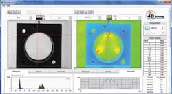
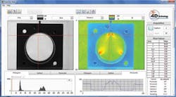
Like Fraunhofer, 4D Technology (Tucson, AZ, USA; 4DTechnology.com) has used a similar principle in the design of its range of PolarCam snapshot polarization cameras. 0, +45 degree, 90 degree and 135 degree polarizing elements with a broad response across the visible spectrum are arranged in a repeating, 2x2 pixel grid across the sensor array. The cameras are available with 0.25, 1, 2 and 4 Mpixel sensors from Truesense Imaging (Rochester, NY, USA; www.truesense.com) and operate at data rates up to 260fps. Optional PolarView software provides real-time display and calculation of key polarization parameters, including the degree and angle of linear polarization.
Adding specialized optics or multiple filters to off-the-shelf photodiodes or CCD and CMOS imagers can also be used to develop multi-spectral imagers. Over two years ago, IMEC (Leuven, Belgium; www.imec.be) demonstrated a multi-spectral imager that effectively replaces the slit and collimator of traditional multi-spectral imagers with a wedge of Fabry-Pérot filters. Placed onto a 4MPixel image sensor, each filter transmits a narrow band of wavelengths and rejects wavelengths outside of that band resulting in a multispectral camera that transmits 100 spectral bands of 5-nm bandwidth at rates of 25 fps (see "Novel sensors help smart cameras serve niches" Vision Systems Design, May 2012; http://bit.ly/1kNZzEV).
Of course, other approaches can also be used to produce lower-cost devices as realized by Pixelteq (Golden, CO, USA; www.pixelteq.com). In the design of its PixelSensor multi-spectral image detectors, the company has chosen to incorporate eight individual photodiodes, each coated with a specific filter to capture images from eight selected bandwidths ranging from approximately 400-700nm.
At Photonics West, the company demonstrated how the company's PixelSensor development kit could be used by OEMs to evaluate the imager. With the image sensor embedded onto the PCB development kit, the board provides eight independent amplification channels and transfers captured data over a mini-USB interface to a host computer. This enables developers to select channels-specific settings, sampling modes and data and display options.
As IMEC has shown, however, such filters do not have to be coated onto the imagers but can be applied optically. Indeed, this is the approach taken by researchers at the Fraunhofer Institute for Integrated Circuits (Erlangen, Germany; www.iis.fraunhofer.de).
Instead of applying optical Fabry-Pérot filters or adding different filters to each individual pixel, an aluminum structure approximately 200nm thick is pattered with an array of holes of a specific diameter and period. Both the period and diameter of these holes affect the peak wavelength and the filter bandwidth of the transmitted light, respectively. For example, with a diameter 200nm and period 320nm, patterned in a 200nm thick aluminum layer, a peak wavelength of approximately 570nm (green) is obtained (see "Nanostructured Optical Filters in CMOS for Multispectral, Polarization and Image Sensors," Microelectronics, p. 9-17; http://bit.ly/1bFkuaw).
By choosing different diameters and periods for this structure, and placing the array onto an imager, different wavelengths and bandwidths can be obtained. According to Dr. Stephan Junger, Senior Scientist at the Fraunhofer Institute, a 12-channel line scan imagers is currently under development and will be demonstrated in a line-scan camera at the forthcoming Vision Show in Stuttgart in November this year.
Vision Systems Articles Archives
About the Author

Andy Wilson
Founding Editor
Founding editor of Vision Systems Design. Industry authority and author of thousands of technical articles on image processing, machine vision, and computer science.
B.Sc., Warwick University
Tel: 603-891-9115
Fax: 603-891-9297

