Vision and scanning probes inspect photomask defects
To check critical dimensions, advanced metrology systems combine visible-light microscopy with stylus nanoprofilometry.
By C. G. Masi, Contributing Editor
As digital-electronics clock speeds advance past 1 or 2 GHz, semiconductor manufacturers have to fabricate chips whose critical dimensions (CDs) are much smaller than a wavelength of light. The active elements in a digital IC are field-effect switching transistors, and the speed at which they can switch goes up as the gate width goes down. The minimum manufacturable gate width thus determines the maximum clock speed. Chipmakers look to semiconductor-manufacturing equipment vendors such as FEI Company to provide tools capable of reliably fabricating these structures.
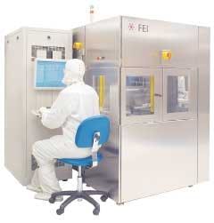
FEI developed a system to allow semiconductor fabricators to accurately measure and inspect masks for the most demanding, small-featured ICs being fabricated. The SNP XT stylus nanoprofilometer uses an automated video microscope to navigate to within 1 µm of the feature of interest, then switches to a stylus nanoprofilometer (SNP) to locate the feature and measure its critical dimensions (see Fig. 1 and "Of SNPs and AFMs" on p. 31).
null
"Our system is in use at almost all the major captive and merchant [semiconductor fabrication] shops in the world for both metrology and repair," says Troy Morrison, senior product manager at FEI. "Most of the photolithography-mask defects roughly 100 nm in size or larger have to be repaired." These photomasks are the templates that define which areas will become transistor gates, for example, and which will be conductors between transistors.
The photomasks that the system inspects are 6-mm (1/4-in.) thick, 150 × 150-mm (6 × 6-in.) quartz plates with lines and features traced out on the surface in optically dense material. The photomasks needed for the finest features use a chrome layer on top of several underlayers of quartz and/or molybdenum silicide to form an interference-filter stack. If a mask has a defect in its CDs, it can ruin thousands of ICs during fabrication.
TAKING THE MEASURE
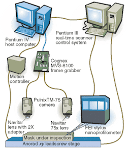
The SNP XT uses its scanning probe microscope to measure CDs at multiple sites across a photomask (see Fig. 2). The procedure starts when a robotic photomask handler places the mask on the inspection system's chuck, which is mounted on an Anorad x-y positioning stage. The low-magnification video microscope consists of a JAI Pulnix TM-75 camera with a 1/2-in., high signal-to-noise-ratio CCD, Navitar Precise Eye right-angle body, 1X adapter, 0.75X complementary lens, and high-brightness red LED light source, and has a 4.7 × 3.6-mm field of view.
FIGURE 2. In the SNP XT, camera outputs feed through a frame grabber into a single-board computer that controls the cameras, analyzes the video images, and communicates with a second single-board computer that operates the mechanical stage and the SNP XT system.
A Cognex MVS-8100 frame grabber captures the image and feeds it into a single-board computer driven by an Intel Pentium 4 processor. The system uses a second single-board computer, this time driven by a Pentium 2 processor, to control the motorized stage and the SNP XT.
The microscope locates three fiducial points marked on the surface of the mask. From the locations of these points, an image-analysis computer calculates the transformation between the machine coordinates and the mask coordinates. It uses the observed distances between the fiducials to calculate a scale factor, the observed position of a coordinate-zero fiducial to calculate a translation vector, and the angles between lines connecting the fiducials to calculate a rotation tensor. With these measurements, it can calculate the machine coordinates of any desired mask coordinate within 1 µm.
The next step is to drive the stage under a higher-magnification camera mounted on the SNP XT head so that it views the first CD measurement location. This high-magnification microscope has a 60 × 80-µm field of view and consists of another TM-75 camera with a 75X Navitar lens, Mitutoyo Infinity-corrected 20X adapter, Navitar Ultrazoom superhigh-resolution coupling lens, short 2X adapter, and high-brightness coaxial red LED illluminator. The same Cognex frame grabber captures images from this camera, as well.
Using a pattern-recognition system, the image-analysis computer identifies the location of the CD withinthe high-magnification camera's field of view. It sends that location to a second computer system, which controls the SNP XT probe manipulator. The system, however, is not yet where it needs to be. The features are barely resolvable using visible-light video microscopes because they are 360 nm across on the mask and need to be controlled to within 2 nm. The pattern-recognition system can identify a location but cannot accurately zero in on it for a measurement. Next, the correct feature is identified by "feel."
"Let's say there's an array of lines and spaces," Morrison explains, "and the customer wants to measure the third line out of the set of five. After the system is driven to the correct stage coordinates, it may be accurate to within a micron. However, the features that we're measuring are often 500 nm or smaller, so the probe would scan in a direction across the lines and the computer would have a recipe to look at the scan, identify where the third line is, and identify it as the object of measurement. The scan amounts to a quick 1-D pattern-recognition algorithm that takes just seconds. That allows the system to isolate the specific area to make the measurement rapidly at high resolution. Its measurements would include the feature height, width, and sidewall angle."
PROBING ISSUES
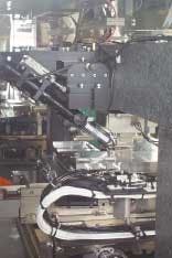
The dimensions that are critical for judging the photomask quality are the height and width of the feature's cross section, along with a measurement of the sidewall angle. To obtain this measurement, the system steps across the flat interfeature surface of the quartz wafer. When it reaches the feature, it begins moving up the side, feeling for the feature's sidewall as it goes. At the top, it again probes for the vertical position of the top. Then it probes down the other side and finally across the flat again (see Fig. 3).
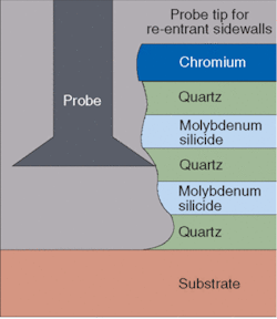
There is no practical probe shape that can cover all surface-feature profiles. For example, the measurement of a deep feature diameter at both the bottom and top of a sidewall is best done with a cylindrical high-aspect-ratio tip. Such a straight-sided tip makes it easy to subtract the tip contour from the raw data. Multilayered photomasks, however, typically present re-entrant wall profiles that a cylindrical probe could not possibly follow. For such features, the system needs a probe shaped like an inverted cone (see Fig. 4).
FIGURE 4. Taking CD measurements of re-entrant sidewalls in advanced multilayer photomasks requires a probe shaped like an inverted cone. Only by having the probe wider at the base than at the top can the system deal with overhanging sidewall structures.
To cover all of the feature profiles in photomasks, the SNP XT carries an onboard library of precharacterized tips for different applications. Automated probe-assembly exchange is facilitated by a simple magnetic attachment to the scanning-probe assembly. The raw data coming from the SNP XT show the position of the probe's center, not the actual position of the surface it is feeling. The SNP XT computer, knowing the probe's shape and which part (flat bottom or cone-base edge) contacted the surface, calculates the feature profile that must have been present to cause that probe-position profile.
When qualifying a photomask, the system will typically make four to 16 measurements of each CD, and look at five to 50 CDs on the mask; there may be dozens of photomasks needed to make a given IC. To drive the system manually would take an enormous amount of time, even if it could be done with accuracy. From that standpoint, there is no alternative to making the measurements with an automated system such as the SNP XT.
While the CD measurement is more interesting from an automated-inspection standpoint, the system can perform other studies automatically, as well. Of equal importance for the semiconductor manufacturer is characterizing photomask defects. The SNP XT can locate a photomask defect (usually a lump of opaque material appended to the side of a feature or of quartz piece lying between features) and characterize it. The resulting map allows a focused ion-beam-milling system to cut away the area, correcting the defect.
features, advantanges, benefits
"Our experience with the SNP 9000 indicates that the SNP XT will be extremely helpful to semiconductor fabs," says Eric Poortinga, senior engineer at Photronics. "We especially like the system's three-dimensional CD measurement capability and the ability to search for specific features. When looking at mask defects, the three-dimensional metrology capability inherent in SNP measurements allows us to determine how critical a given defect is. We can then judge whether or not it will be necessary to repair that defect.
"Many of our customers specify exactly which features they want us to measure at different locations on the mask. The system's search scanning feature makes it possible for us to assure those customers that we actually are measuring the critical dimensions of the features they want measured, and not something else."
Of SNPs and AFMs
A stylus nanoprofilometer (SNP) is a microimaging device that is, in many ways, very similar to an atomic-force microscope (AFM). The main difference is that, while the AFM uses atomic-level forces (Van Der Walls forces) of about 25 nanoNewtons (nN) to locate the edge of an atom, the SNP actually contacts the surface being studied with a force on the order of 100 nN. Bringing the probe into contact with the surface allows it to make more accurate critical-dimension (CD) measurements than it could if it hovered over the surface, balanced on an atomic-force cloud.
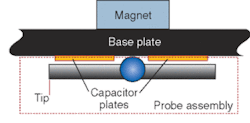
The force sensor is a compact (10 × 5 mm) silicon balance-beam assembly with an attached probe and tip and integral capacitive sensors for force and location detection. The assembly pivots on a pair of precision ball bearings. A piezoceramic scan actuator attached to the base plate positions the assembly with respect to the feature to be measured. Position is sensed in x, y, and z axes by three sets of capacitance sensors (see figure).
SNP uses an electrostatically located balance beam to sense probe forces. The beam itself is free to rock on low-friction bearings. Capacitive elements over each beam end sense its position and apply electrostatic forces. A feedback system controls the capacitor voltages to hold the beam level against the probe force. Sensing the feedback voltage provides an output signal proportional to the probe force. The whole assembly attaches to the SNP XT via a magnetic clamp.
During a measurement, an electronic control system keeps the beam balanced by applying voltages to the capacitor plates. When the force that the sample surface exerts on the probe tip upsets the balance (typical force sensitivity <50 nN), the system senses the inbalance and alters the capacitor-plate voltages. This action modifies the electrostatic forces to re-establish beam's balance, keeping the probe tip at a fixed position relative to the base plate and scan actuator.
The rebalancing voltage needed is directly proportional to the surface force. By moving the tip into the surface until the rebalancing voltage reaches a preset level, then recording the capacitive sensors' outputs, the system can map the surface topography to within 0.5 nm.
C. G. M.
Company Info
Anorad Shirley, NY, USA www.anorad.com
Cognex Natick, MA, USA www.cognex.com
FEI Company Hillsboro, OR, USA www.feicompany.com
JAI Pulnix Sunnyvale, CA, USA www.pulnix.com
Mitutoyo America Aurora, IL, USA www.mitutoyo.com
Navitar Rochester, NY, USA www.navitar.com
Photronics Brookfield, CT, USA www.photronics.com

