Thin-film solar cells tested using InGaAs SWIR camera
Electroluminescence analysis accelerates development and improves quality
By Raf Vandersmissen, SinfraRed
Copper indium gallium diselenide (CIGS) thin-film cells for solar energy generation offer decisive economical advantages by enabling lightweight and flexible modules. They consume less energy and fewer materials in their fabrication and yield good energy levels across a broad spectrum even in unfavorable weather conditions. Analyzing their inherent near-infrared electroluminescent radiation with sensitive InGaAs shortwave infrared (SWIR) cameras allows a detailed structural examination to shorten the development cycle of new module types and support module manufacturing through components and facilities that result in high reliability, high efficiency, and long-term operability.
The technology of CIGS thin-film solar cells
Thin-film solar cells are made of semiconductor layers measuring just a few microns thick. This enables their integration in functional and decorative building elements such as roof shingles and roofing tiles, as well as entire facades of buildings, glass domes, and air wells. Solar-enabled roof shingles, of course, should offer the same degree of weather protection and durability as those made of traditional bitumen. This opens up new methods of energy generation, not just on saddle roofs but also on different roof shapes.
Among the materials currently used for thin-film cells are crystalline silicon (Si), CIGS, or gallium-free CIS, as well as cadmium telluride (CdTe). All of these already offer interesting market opportunities today. Long-term success, however, will depend on achieving higher efficiency and lower cost.
As a detriment to thin-film solar cells, not much is known yet about their behavior under various light and weather conditions when compared to cells and modules made of crystalline silicon, which have reached impressive maturity over the last 25 years. There are, however, very powerful and meaningful test methods that have become available for a detailed structural investigation of thin-film modules, which can substantially accelerate their market introduction and improve manufacturing quality.
Electroluminescence -- a weak but meaningful effect
One of the most important phenomena occurring in all functional photovoltaic cells is the weak electroluminescence (EL) emitted by them, caused by an external bias voltage. A solar cell can be regarded as the parallel interconnection of numerous p-n junctions. Into these p-n junctions, the external bias voltage injects electrons, which in part recombine with the available holes. The surplus energy exits as photons whose wavelength depends on the bandgap of the cell's absorber material.
Below is a summary of the correlation of bandgap energy and wavelength of the resulting electroluminescent emission in four commercially available solar cell types. For comparison, the spectral coverage of a VISWIR camera in InGaAs technology is also shown. CIGS thin-film modules have bandgap energies from 0.9 to about 1.7 eV, depending on the ratio of indium and gallium. A higher share of indium will lower the bandgap energy; more gallium will increase it.
Properties of commercial materials for thin-film solar cells
CdTe
- Material: Cadmium telluride
- Bandgap (eV): 1.4
- Wavelength (µm): 0.8
CIGS
- Copper indium gallium diselenide
- 0.9 to 1.7 (depending on the ratio of indium/gallium)
- 1.3 to 0.7 (depending on the ratio of indium/gallium)
CIS
- Copper indium diselenide
- 0.9
- 1.3
VISWIR camera
- InGaAs technology
- 0.4 to 1.7 (wavelength)
The wavelengths of the ensuing electroluminescence then range from 800 to about 1200 nm. This exactly happens to be the spectral area in which SWIR image sensors show their largest sensitivity. To cover even larger bandgaps well into the visible realm and enable parallel imaging in the visible and the IR areas, image sensors are tending to larger bandwidths. With appropriate constructive measures, this yields VISWIR sensor arrays with a high spectral sensitivity at wavelengths between 0.4 and 1.7 µm.
The intensity of a solar cell's electroluminescent emission is determined by the concentration of electrons and holes, which increases exponentially with bias voltage as expected from the regular I-U curve of a diode. Thus, measuring the EL emission intensity of a solar cell will yield valuable, spatially distributed details of mechanisms that could substantially diminish the power yield of a solar module. Among the causes are locally reduced diffusions lengths, microfissures within the cell, parallel-resistance effects, and contamination of the semiconductor layers.
A look at the cross-section of a CIGS thin-film solar cell monolithically connected in series to the neighboring cell (see Fig. 1) reveals three critical areas that might be affected by humidity penetrating under the transparent and conductive oxide layers (TCO) and thereby diminishing the cell's properties. First, in the area marked P1, there is a lowered parallel resistance (shunt Rsh). Second, at P2, there is a corroding ZnO/Mo contact. Third, at P3, there is a rising series Rs due to corrosion of the molybdenum layer. All these effects may at some point cause a significant loss of power.
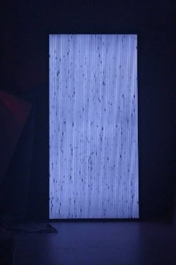
As can be seen in the electroluminescence image (see Fig. 2) of a CIGS module, the method described here enables a quick and accurate diagnostic of the module as a whole. This can be of utmost value in research and development as well as in the production of thin-film modules.
SWIR imagers in InGaAs technology
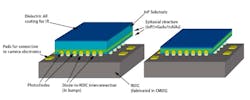
Figure 3 shows the structure of an SWIR InGaAs imager for a wavelength area 0.9 to 1.7 µm (left). The IR photodiodes are built on an InP epi-wafer substrate that is usually more than 125 µm thick. Since this technology is not particularly well suited for realizing readout circuits, the photodiode array, together with its read-out integrated circuit (ROIC), is flip-chip mounted via indium bumping on a CMOS chip. The solar cell's exposure is then fashioned from the back, through the substrate. This, however, absorbs all light from the visible realm to 0.9 µm.
To prevent this loss of light, the substrate is thinned after the flip-chip mounting step as is routinely done in standard InGaAs sensors to improve response, but here it is applied in a more thorough way. To be able to safely remove the substrate without damaging the InGaAs detector, additional layers of InGaAsP are inserted just below the photodiodes. They function as etch stops within the InP area. An HCL etch then selectively removes the InP epi-substrate exactly up to the InGaAsP etch stop layer. This effectively thins the sensor chip down from 125 µm to just 5 µm (see Fig. 3, right), making it transparent to light in the visible realm and opening up the sensor to a broad wavelength coverage from 0.4 µm to 1.7 µm.
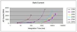
The observed electroluminescent emission is of very weak intensity. This puts strict requirements on the measuring technique used. Accurate measurements will necessitate long integration times. In this regard, the dark current of the image sensor is setting a limit. This can be detrimental, especially when carrying out more accurate examinations in the design of novel photovoltaic cells and modules. Dark current can be reduced by employing low-noise sensors, as in the Xenics XEVA camera, and by one- or multistage thermoelectric cooling of the sensor array (see Fig. 4). This will enable a 100-fold longer integration time and prevent weak local imperfections from getting unnoticed in the noise floor.
Meaningful measuring results
Figure 5 clearly demonstrates the significance of electroluminescent radiation in the near-infrared as captured by an SWIR camera. At the outset of a corrosion test (left), the module still radiated across the entire surface. After an extended hot-steam treatment over 1000 hours, the sample suffered -- obviously due to its sub-optimal mounting -- substantial TCO corrosion along the edges (right). The lowering of the shunt resistors Rsh, plus rising series resistances Rs, practically cut the cell's power yield in half.
Conclusion
An analysis of the weak electroluminescent emission given off by photovoltaic cells and modules using sensitive infrared cameras substantially supports the development of thin-film solar cells, as well as their integration in functional carrier structures and quality assurance during manufacturing. This will serve the overall goal of reducing the historical lead of traditional solar cells in favor of thin-film cells and developing novel power supply solutions based on freely available solar energy.
Raf Vandersmissen is CEO of SinfraRed (Singapore; www.sinfrared.com), a spinoff of XenICs NV (Leuven, Belgium; www.xenics.com).


