Solar Scribing
Winn Hardin, Contributing Editor
Although not yet as efficient at converting light into electricity, thin-film solar panels are expected to eventually overtake their silicon-based competitors because thin-film panels can be less expensive to manufacture and do not require increasingly scarce silicon crystals. A machine-vision system incorporating four scanner stations offers the potential of ensuring quality during the laser scribing and coating of the panels.
Thin-film solar panels are constructed in a similar method to semiconductor chips. Transparent semiconductor oxide (TCO) glass, instead of silicon wafers, provides the base substrate to which various optically active and conductive films are applied. In between deposition steps, lasers scribe a variety of lines—P1, P2, and P3—on the TCO glass.
P1 laser scribe processes use 1064-nm pulsed lasers to pattern the whole TCO glass panel into individual cells; P2 laser scribe processes use 532-nm lasers to remove absorber layer material to allow formation of cell interconnects; and P3 laser scribe processes uses 532-nm lasers to isolate each cell formed by P1 and P2 scribe lines.
Typically, the TCO glass is washed and then inspected for glass defects, TCO coating defects, warpage, washer debris, edge cracks and chips, corner breaks and flares, and panel length, width, and squareness just after entering the thin-film solar plant. Then P1 scribe lines are created; P1 scribe lines are inspected by collecting images of sections of the scribe line and looking for defects while measuring the scribe width.
Another coating is applied; the coating is inspected; then P2 lines are cut into the surface of TCO glass and these scribe lines are also sampled. Finally, another coating is applied and P3 scribe lines are created and a final inspection conducted before the panel moves to the packaging area.
Traditionally, machine vision has helped thin-film manufacturers maintain quality by using brightfield imaging systems with area-array CCD cameras to sample portions of the scribe lines and glass coatings after each step. These inspections help keep the manufacturer from adding value to defective product, and maximize the usable area of each piece of TCO glass, thus increasing overall equipment effectiveness (OEE) and productivity. However, these camera systems have not been used to inspect 100% of the TCO glass or scribe lines because of the difficulties in locating defects of a few microns with sufficient speed and tolerance to panel warp and bounce to meet production throughput.
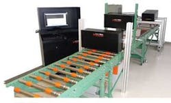
Recently, a US manufacturer of cadmium telluride (CdTe) thin-film solar panels turned to glass inspection specialist Dark Field Technologies to build a system capable of inspecting TCO blanks as well as 100% of the three scribe lines. Dark Field complied by supplying washed glass inspection systems, and darkfield scribe-line imaging systems. The company adapted its NxtGen imaging system to the task, using DALSA Piranha2 dual-tap, 8k-pixel linescan cameras purchased from distributor 1stVision connected to a Matrox Imaging Helios image-processing frame grabber housed in a Dell work station (see Fig. 1).
null
Away from the light
The inspection of scribe lines and associated defects are critical to an efficient thin-film solar cell. These scribe lines may be only 40 µm wide. Conventional metrology systems utilize area-array cameras to produce snapshots of very small sections of the solar panel—less than 0.2% of the surface area. These systems cannot tolerate glass bounce or warp and must perform the inspection at slow speeds.
Dark Field Technologies uses linescan cameras to capture 100% of the TCO glass surface with darkfield, brightfield, or a mix of imaging modalities, depending on the application. Darkfield imaging positions the light so that it will not be reflected or transmitted back to the camera; brightfield imaging captures reflected or transmitted light.
“It’s the nature of the defects that define your optical system,” explains Timothy Potts, president of Dark Field Technologies. “If you have defects that change the amount of light that is reflected or transmitted, then the defects act as brightfield events. But if you have defects that change diffusion or diffraction of energy, those are darkfield events. If you have something that’s very clear or highly reflective—like glass—and you have diffractive defect, you don’t see it in a brightfield image.”
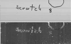
He adds, “A scratch is classic darkfield event. If you’re in a dark room and you hit a scratch with laser, it scatters light everywhere. A brightfield vision system can’t see that scratch” (see Fig. 2).
The cameras are mounted in parallel to capture an image of the 24-in. wide TCO float glass as it passes underneath the scanner following the glass washer. The first scanner works in brightfield mode, capturing images of reflected laser light from four individual laser point sources spread across the width of the TCO glass.
The image data are fed line by line across Helios Camera Link frame grabbers with on-board image processing and memory buffer housed in a Dell T7400 multicore processor work station. In the work station memory, each pixel value is compared to neighboring pixel values to identify the bright laser reflections at rates of 500 million pixels every three seconds thanks to the Helios/work station processing combination.
If the glass is warped, the reflections will appear to move in relation to the sensor’s field of view. The amount of warp is determined by triangulating the position of the reflected laser light in relation to the known location of the camera and laser illuminator.
“The glass that comes in isn’t flat,” says Potts. “As you go from annealed to tempered, the warp gets worse and worse. As you scribe it, you increase the glass temperature further and the warp may increase. As it gets more warped, you lose the ability to scribe it with the laser because you’re out of the depth of field of the laser scribe. So it’s imperative to measure the warp, at least the beginning, and preferably after all three scribe lines, too.
“Before the semiconductor coating is applied,” he adds, “we can measure to either the front or the back of the glass surface. After it’s applied, we can only measure from the clear side of the glass, but that’s really all we need—just one surface.”
Down in the dark
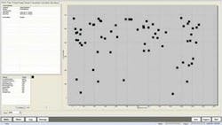
Because darkfield imaging uses the absence of light rather than a changing grayscale intensity value, it yields high-contrast images of defects. However, this advantage has kept darkfield imaging from industrial environments where a speck of dust can be misconstrued as a defect. “Which is why we inspect the glass for warpage immediately after it comes out of the washer, and for the scribe lines right after the glass comes out of the scribing station just after the semiconductor deposition, which happens in a clean environment,” says Potts (see Fig. 3).
Darkfield imaging techniques allow the scanner to capture defects as small as a few microns with sensor pixels that are 7 μm2. “We can use an optical pixel that is much larger than the defect of interest. And because we’re using an optical pixel that is larger than the event that we’re trying to detect, that gives us a larger depth of field. And that large depth of field gives us tolerance to the glass panel’s unevenness, warpage, and vertical bouncing as the glass passes over the conveyor,” Potts explains.
As the glass exits the P1 scribe station and before the semiconductor coating is applied, Potts team inspects the panel using a darkfield transmission approach where a 24-in., red-LED-source fiberoptic line light from Fiberoptics Technology is placed behind the translucent glass to enhance the P1 scribe line as it refracts and diffuses the light away from the camera. “LEDs will give you light, but they don’t give you directionality. Fiberoptic line lights are nice thin, directional lights,” says Potts.
“The current concept was born from our decades of laser system design experience with float glass and coated glass. Closely controlled illumination is critical to create a stable darkfield optical system. A laser system is an ideal darkfield machine, but the costs are prohibitive in solar thin-film production, and there are challenges related to fringes created by the laser light diffraction.”
Image data from the two Piranha2 linescan cameras are fed via Camera Link to the Helios frame grabber and analyzed using a normalized correlation, pixel-to-pixel algorithmic approach to detect the smallest defects along the P1 scribe line, as well as measure the width and position of the 40-μm-wide scribe line with ±5-μm precision.
After P1 scribe inspection, the CdTe active semiconductor thin-film layer is deposited in a cleanroom environment. The glass then goes to the P2 laser scribe station and is subsequently inspected by a third NxtGen system, operating in darkfield reflection mode because of the opaque semiconductor film.
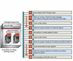
“All the scanners are the same, but we configure them differently,” adds Potts. “We use darkfield transmission on P1 scribe line inspection, and darkfield reflection on P2 and P3 because of the opaque semiconductor coating. Using our proprietary optics, we can see both the P2 and P1 scribe lines, which allows us to check the offset between the two as well as find defects along the P2 scribe line. After the P3 scribe line is created, we do a final inspection, and again check offsets between P2 and P3, as well as look for defects along the P3 scribe line (see Fig. 4).”
Offsets are important because the mission is to maximize the usable area of the coated glass. Potts says, “Offsets and scribes are dead zones that don’t produce electricity. While it is possible to image P1, P2, and P3 at the P3 station, the optical system is unstable; it cannot give consistent results on line. Again, a laser system performs superbly, but the costs are prohibitive.”
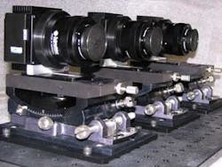
Each scanner consists of two cameras, an illuminator, and a goniometer to set the angle between the camera and light (see Fig. 5). “We’ve applied for a patent for a variable-field scanner design that will allow us to go from darkfield to brightfield to a mix of both automatically,” Potts says. “Right now, you have to make the adjustments manually.”
While critics might say such functionality would be good for designing and beta testing an application but not for volume deployment, Potts counters that the majority of time spent in glass inspection is set aligning the light to the camera and glass surface to get a good image. This is particularly important in applications where a change in product or coating should be accompanied by a change in the optical field. Automating that process would cut significant engineering time out of the equation, improving the customer’s rate of return on their investment.
Company Info
1stVision, Andover, MA, USA
www.1stvision.com
DALSA, Waterloo, ON, Canada
www.dalsa.com
Dark Field Technologies
Orange, CT, USA
www.darkfield.com
Dell, Round Rock, TX, USA
www.dell.com
Fiberoptics Technology
Pomfret, CT, USA
www.fiberoptix.com
Matrox Imaging
Dorval, QC, Canada
www.matrox.com/imaging
