Next-Gen Contact Image Sensors Enhance Inspection of Batteries and Printed Material
Contact image sensors have come a long way. The latest generation of this technology provides higher speed, resolution, and dynamic range than its predecessor.
These improvements make contact image sensors (CIS) suitable for inspection and metrology tasks in spatially restricted machine vision environments, such as battery production and printing lines, where precision and efficiency are essential.
This article will examine the challenges of inspecting battery and print materials and how CIS technology offers an optimal solution. One advantage of CIS technology is its compact form factor compared to conventional line scan cameras. While conventional systems typically require a working distance of 250~500 mm, CIS operates within just 10~20 mm. This makes CIS ideal for use in spatially restricted in-line automatic optical inspection (AOI), which is essential for real-time, high-throughput quality control. CIS is also highly integrated, combining the camera, lens, and lighting into a single unit, which simplifies system design and speeds up installation. Due to these benefits, CIS is increasingly being adopted in machine vision applications.
Enhancing Lithium-Ion Battery Production: The Role of CIS in Precision and Automation
Clean energy programs worldwide are driving the transition from vehicles with internal combustion engines to electric vehicles (EVs). This requires scaling up the production capacity of lithium-ion batteries (LiBs), the core of electric vehicle technology. Automation plays a key role in achieving the required economies of scale for lithium-ion battery production.
One of the most important parts of lithium-ion battery manufacturing is the battery electrode manufacturing process. This involves multiple stages of coating, calendering, slitting, winding, packaging, etc. depending on the type of battery, such as cylinder, prism, or pouch. Speed is 50~80m/min, film thickness 50~100 µm with variation ±5~25 µm. Common fields of view in production lines are 400, 700, 800, and 1500 mm. Optical inspection with an object resolution of 15~30 µm is used to detect defects such as pinholes, cracks, scratches, delamination, leakage, etc. Besides, measurements of film thickness, width, edge, positioning, etc. are required to deliver feedback to the control loop. All these tasks can be done using small form factor CIS modules that fit into the restricted space in the production machines. Advanced CIS technology, with 120 kHz, 900 dpi, and true metrology has become an enabler for the real-time quality control of the electrode manufacturing process today. High dynamic range imaging also helps to capture clear images of dark graphite materials coated on highly reflective copper foils.
Related: Contact Image Sensors Challenge Linescan Cameras
Lighting is another important part of the vision system, and either internal or external lighting can be used. Many applications use brightfield configuration at an angle within ±30° off the axis perpendicular to the web to achieve the required image quality. Strobed light can also be used to capture multifield images that effectively help to identify certain defects.
Print Inspection: Leveraging CIS Technology for Compact, High-Accuracy Systems
Print inspection is another application that benefits from the use of CIS. Compact-size print inspection systems are becoming popular for printed labels and packages. These small systems cannot use conventional vision systems with line scan cameras for obvious reasons. CIS provides an ideal solution, which in general requires color inspection with a relatively larger pixel size of 50~250 µm. Common fields of view are 500, 600, and 1100 mm.
The newest CIS technology uses trilinear CMOS sensors coated with dye-based RGB color filters. The trilinear sensor captures true RGB colors with a max line rate of 60kHzx3. To combine three colors into a full-color image, spatial correction is required. Spatial correction is automatically done in the module even with the stagger sensor architecture, usually by buffering the first and second channels to match the third. All of these elements combine to result in high-color fidelity images that capture every detail.
Related: What's the Optimal Assembly Verification Method for Tough Inspection Tasks?
Lighting is a key part of print inspection as well. To detect faint colors, a white LED light source is chosen with a strong yellowish component. For LED light, color temperature using the blackbody radiation model does not work well. Therefore, end users need to specify spectral characteristics that fit into the inks used in the prints.
Enhancing System Throughput with High Speed and Resolution
In vision systems, speed and resolution are essential specifications, but they often limit the capabilities of current CIS products. To overcome these challenges, the next generation of CIS technology must improve imaging performance. For example, in battery production lines—critical to the clean energy shift toward EVs—automatic optical inspection systems require both high speed and resolution to meet throughput demands. By integrating smaller pixel sizes with faster line rates, CIS technology can ensure high detectability while maintaining system throughput.
Greater resolution not only increases detectability but also boosts measurement accuracy. Figure 3 demonstrates the difference in measured Modulation Transfer Function (MTF), mean values, and standard deviations for black-and-white line pair targets at 45 µm/line and 500 µm/line, comparing 900 dpi with 600 dpi. Although 600 dpi is the standard in most CIS modules, accuracy improves by nearly 50% when using 900 dpi.
|
28µm (900dpi) |
42 µm (600dpi) |
||
|
MTF (target 45 µm/line) |
40.9% |
27.6% |
|
|
Measurement (target 500 µm/line) |
Mean value |
501.2 µm |
504.8 µm |
|
standard deviation |
5.928 µm |
13.33 µm |
|
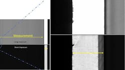
Another way to achieve dynamic range is to use a dual-line sensor with independent exposure control in monochrome mode. This approach captures both bright and dark areas in a single scan by applying different exposures to each line. The two images captured can either be processed separately or combined into one HDR image for further analysis. This approach has proven effective, particularly when imaging dark electrodes on highly reflective metal rolls, greatly enhancing detectability in varying lighting conditions.
Metrology: Achieving High Accuracy Without Missing Pixels
A key advantage of using CIS technology is its telecentric self-focus lens, which ensures undistorted, 1:1 optical magnification for precise metrology in addition to defect detection. Many current CIS modules on the market rely on a butting process to join individual silicon dies. This method often leads to small, uncontrollable gaps between the dies, resulting in missing pixels. To address these gaps, data interpolation is typically used, but this process can lead to inaccurate data and inconsistencies in sensor width, especially when the manufacturing process is suboptimal.
Related: Keys to Deploying Machine Vision in Precision In-Line Measurement Applications in Manufacturing
A better approach is to use staggered CMOS sensor architecture. This design eliminates gaps between the silicon dies, ensuring full coverage of the field of view (FOV) without missing pixels. The image processing within the module aligns the images from each die and removes any overlap, allowing for true metrology applications with precise horizontal measurements. After calibration, this setup can achieve an accuracy of around 50 µm at a 20°C ambient temperature over an 800 mm FOV.
Unlike traditional line scan cameras, a CIS is positioned very close to the samples being inspected, making dust protection critical. Therefore, it is essential to select a CIS with an IP60 rating for its optical path to prevent contamination from dust in the inspection environment.
Conclusion
While initially developed for consumer electronics like printers and scanners, Contact Image Sensor technology has found its place in machine vision, where its applications continue to expand. As industry demands increase, CIS technology will evolve to achieve faster speeds and higher resolutions. In addition, the need for extended working distances and deeper depth of field will grow, allowing for more advanced multifield lighting techniques. Multispectral imaging will also become increasingly important for certain materials. By incorporating these advanced features, the industry will be able to address more complex challenges, driving the development of higher-value solutions for a wide range of applications.
About the Author

Xing-Fei He
Xing-Fei He, PhD, is a senior product manager at Teledyne DALSA (Waterloo, Ontario, Canada), a part of the Teledyne Vision Solutions portfolio. He has managed multiple CCD and CMOS product lines at the company and is responsible for product planning, development, rollout, and marketing and sales of these products. He helps to define product strategies, champion technical marketing and sales, and build channel and OEM relationships.


