Vision retrofit inspects microcircuit boards
Off-the-shelf camera and autofocus system work with adaptive control software to optimize throughput despite warp.
By R. Winn Hardin, Contributing Editor
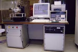
Retrofitting a manufacturing line is a daunting task for a system designer. The customer wants to reuse as much equipment as possible, and constraints on hardware placement and size can mean the solution will require new methods to accomplish the task. Metrigraphics, a division of Dynamics Research Corp. that manufactures microcircuit boards for a variety of applications, called on Mnemonics Inc., a vision-system-design and integration company, to rebuild a system for defect inspection (see Fig. 1 on p. 54).
Metrigraphics has used vision systems for automated inspection of 12- to 60-µm-diameter holes in microcircuit boards for several years, but a new product line required trace and defect inspection of printed substrates up to 12 × 12 in. with minimum 1-µm resolution on materials such as transparent and flexible Kapton, ceramic, and silicon. Mnemonics’ solution used a standard 640 × 480-pixel B/W camera with A/D frame grabber, a closed-loop autofocus optical system to counter warp in the substrate while still allowing high-resolution imaging, a pair of direct/reflection and transmission lighting systems to handle the different substrates, and a separate workstation for image processing, freeing up the primary host to gather the 8-Gbyte images of each PCB.
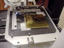
According to Metrigraphics operations manager Doug Hayes, the microcircuit trace inspection system already had an Andor x-y stage to support and manipulate the microcircuit array. Starting at the servos that controlled the x-y stage, the system needed to be rebuilt to meet the 2-pixel/1-µm defect requirement and perform edge detection and area measurements of the trace with a minimum 5-µm line/space periodicity (see Fig. 2 on p. 54).
After reviewing several thousand pictures of microcircuit boards as they came off the production line, Mike Negin, Mnemonics president, determined that he could meet the spatial-resolution requirements within the mechanical limitations imposed by the retrofit. A linescan camera would not work because of the conflicting requirements of large scan areas and the optics required to resolve 1-µm defects. Hayes’ spatial-resolution requirements meant that the average circuit-a plate holds ~90 microcircuits-would have to be broken down into 270 zones (90 circuits × 270 zones = 24,300 fields of view × 0.33 Mbytes = 8 Gbytes/plate).
Simply adding a high-resolution camera with standard optics would not work because the warp of the substrate could mean that portions of each zone could be out of focus, resulting in false negatives. “The substrate and table were flat, but not flat enough to stay in focus,” Negin explains. The best solution was to use an inexpensive sensor and high-power optics with adaptive control software to optimize throughput despite plate warp.
warp correction
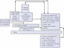
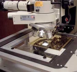
Negin designed a system that mounts a standard Hitachi 640 × 480-pixel gray-scale camera on an Axsys Technologies laser-scan autofocus system (see Fig. 3). The autofocus system includes four motorized microscope objectives and a 5-µm-wide IR laser linescanning system to determine the focal length between the microcircuit cell and the focusing objective/sensor.
Autofocus systems pose challenges for machine vision. At very high resolutions, the field of view (FOV) needs to include sufficient texture to provide the system with enough data to properly focus, which can be challenging for planar-electronics applications. The position of the laser line from the autofocus system also must be carefully placed on the plate, otherwise the 5-µm line can be wider than individual features on the plate, resulting in poor focus. Designers have to engineer moving optics for backlash and overshoot when integrating this type of optical element. Status information from the autofocus unit is monitored by the main PC to guarantee that stable focus is achieved throughout the inspection process, Negin explains (see Fig. 4).
Negin used white LED lights because microcircuit boards have a variety of colored markings, and a single-color LED would filter out markings of the same color. An array of Metaphase Technology white LED lights was connected to the microscope autofocus through a side port and internal prism, aligning the light with the optical axis of the imaging system; the PC controls the illuminators via an RS-232 ports. A second array placed under the Anorad stage provided backlighting for clear, Kapton-based boards that are used for flexible electronic circuits.
The Hitachi camera connects to the PC host (1-GHz Pentium 4 processor, 1-Gbyte RAM) through an entry-level CyberOptics Imagenation PXR board memory and basic camera-control feature set. A Keithley Instruments DAS-series digital I/O board controls the LEDs through a parallel interface, while a separate PCI board controls the Anorad precision x-y stage.
image collection and processing
As each image is collected, it is fed to the main PC host and stored on the hard drive in a specially developed image file that optimizes access. For each of the numerous individual circuit devices on the substrate, hundreds of snapshots of different regions in the circuit are piped to a mosaic image structure designed for rapid storage and retrieval (image files are ~90 Mbytes for each device). After the entire board has been scanned, the complete image is fed across a GigE connection to the nearby Kontron America industrial workstation, also powered by a 1-GHz, P4 microchip and supported by a large hard drive and 1 Gbyte of RAM.
This workstation checks each image against a stored “golden part.” The process begins with a correlation function at the outer edges of each cell for alignment purposes and then shifts to a modified geometric search algorithm to accommodate skew, rotation, and scale changes caused by substrate warpage in the critical interior of the cell. For each FOV and illumination, the system performs a flattening operation to correct for illumination nonuniformity, while bandpass spatial-filtering operations firm up the edges of each trace and relax the edge sensitivities, according to Negin. A segmentation algorithm defines foreground from background, while the defect classification decision uses a context-sensitive blob analysis that integrates the foreground and background information, nearness to edge locations, and proximity to other blob regions.
Using images of existing microcircuit boards and image-processing algorithms to correct for alignment of each cell with overlap, warp correction, and illumination correction, Negin designed the system to create its own golden-part description. This allows the end user to adjust each cell for “sensitivity,” or the allowable variation in characteristics for each cell.
For wide cells with wide traces and broad spacing between traces, Metrigraphics’ Hayes can relax the design criteria for inspection. The result is optimized throughput. According to Hayes, a single board takes an experienced worker three to four hours to manufacture and the inspection system about two hours to inspect.
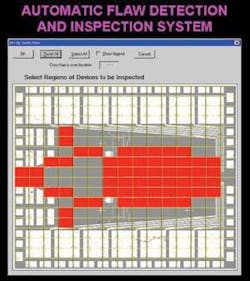
After inspecting the board, the system creates a graphic map that shows each microcircuit (see Fig. 5). Circuits with defects are highlighted in red and then displayed for the operator to review. By clicking on each red circuit, the operator can view potential defects and quickly determine whether a break in a line is a speck of dust or a real defect. Hayes estimates that this process takes 20 minutes and results in a product map that Metrigraphics can ship with the full plate to the end user, ensuring that customers get 100% functional product and guarding against excessive rework or returned orders.
Features, advantages, benefits
“Mnemonics delivered an inspection machine with almost all of the capabilities required in our original design goal and specification,” says Doug Hayes, operations manager at Metrigraphics. “We are very pleased with the machine performance. It has been in production for three years, often running two shifts. We have never had our customer reject a circuit inspected on the vision system.
The vision system can deal with a wide variety of substrate materials, both flexible and ridged, he adds. Once trained, production people can remove and set up the next circuit in five minutes. Teaching the vision system a new product takes about two man-hours and about four machine-hours. Hayes notes, “A very important part of this project was the ease of working with Mike Negin and his team, which delivered a machine that met our requirements for performance and ease of operation.”
Company Info
Anorad,
Shirley, NY, USA
www.anorad.com
Axsys Technologies,
Rocky Hill, CT, USA
www.axsys.com
CyberOptics Semiconductor,
Beaverton, OR, USA
www.imagenation.com
Hitachi Denshi America,
Wadsworth, OH, USA
www.hdal.com
Keithley Instruments,
Cleveland, OH, USA
www.keithley.com
Kontron America,
San Diego, CA, USA
www.kontron.com
Metaphase Technologies,
Bensalem, PA, USA
www.metaphase-tech.com
Metrigraphics Div. of Dynamics Research Corp.,
Wilmington, MA, USA
www.drc.com/metrigraphics/metrigraphics.htm
Mnemonics Inc.,
Mt. Laurel, NJ, USA
www.mnemonicsinc.com
