Digital cameras
Digital cameras
By Yvonne Carts-Powell, Contributing Editor
"Buying a solid-state camera," says Bill Reilly of Datacube (Danvers, MA), "is still a black art." The number of pixels in a two-dimensional (2-D) array is not standardized, nor is the array size. Different manufacturers create devices in which an individual pixel`s area, shape, and center-to-center distances vary. Different architectures are used by charge-coupled devices (CCDs) to provide higher fill rates or faster image acquisition. Because such devices are at the heart of every digital camera system, understanding CCD specifications becomes important when choosing a camera.
For the developer of high-speed digital cameras, the choice of imager type directly affects the circuitry required to build the camera (see "Looking at CCD specifications," p. 62). To increase the data rate from such devices, CCD developers use multiple outputs (or taps). Breaking the analog bandwidth into a number of components lowers the analog bandwidth per tap and allows data to be read at a faster rate. Increasing the number of channels read out directly increases the bandwidth and speed of CCD-based camera systems.
This approach increases the number of output channels, so each channel must be precisely balanced and maintained to produce a uniform image. Thus, high-speed digital cameras will often contain more analog signal-conditioning circuitry than their analog counterparts and will therefore be more expensive. However, because CCD clock control, offset, gain, clipping, and data conversion are performed in the camera, such devices can provide adjustable shuttering, offer low signal-to-noise ratios (S/Ns), and can often be used at large distances from such image-processing equipment as frame grabbers.
Two, four, and more
Providing a camera with 60 frames/s at 648 ¥ 484-pixel resolution and an electronic shutter to 1/100,000 second was the goal of Chris Krialy at Wintress Engineering (San Diego, CA). And, because the camera design had to withstand hostile environments, digital data had to be transferred up to 300 ft at rates of 330 Mbit/s.
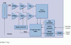
For the CCD at the heart of the company`s OPSIS 3100A digital camera, Krialy chose the KAI-0310 from Eastman Kodak Co. (Rochester, NY), a 648 ¥ 484-resolution frame-transfer CCD with 9 ¥ 9-µm pixels and a dual-tap readout (see Fig. 1). To adjust offset, gain, and clipping from the device, the design uses three op amps that are digitally controlled from an Altera field-programmable gate array (FPGA). "By using a programmable device within the camera," says Krialy, "we make sure both channels are at the same value before they are digitized." Two 8-bit analog-to-digital converters (ADCs) from Analog Devices (Norwood, MA) are used to digitize the video at 16.67 MHz before outputting the data to the FPGA.
"While the FPGA is mainly used to control the clocking of the CCD," says Krialy, "it also acts as a controller for the HOTLink chip. Controlled by the FPGA, the HOTLink integrated circuit built by Cypress Semiconductor (San Jose, CA) is a point-to-point communications link that allows image data to be transferred at 330 Mbyte/s. The HOTLink receiver in the OPSIS 3100A camera accepts digital data from the FPGA at 330 Mbit/s and outputs a 33-MHz clock and a byte-wide data stream for input by Wintress`s own PCI-based digital frame grabber or image processor.
Because Wintress chose a digital approach in the design of its camera, the camera can be controlled digitally over an RS232 serial link. This allows the Altera FPGA to control clocking on the Kodak KAI-0310 so the camera can perform multiple exposures on the same frame with shutter speeds as high as 1/100,000 second.
Trading speed for resolution
Because digital cameras are programmable, the systems developer can often trade resolution for speed. In the design of the Wintress OPSIS 3100A, speed can be traded for resolution--the camera can run at a maximum frame rate of 1200 frames/s at 128 ¥ 128 resolution. Often, however, 128 ¥ 128 resolution is not enough. And to meet these needs different device types must be matched with different camera circuitry.
In the design of its KineView High Speed Video camera, Fred Heuttig`s task at Advanced Optics Associates (AOA, Cambridge, MA) was to build a camera capable of digitizing 256 ¥ 256-resolution images at 1000 frames/s.
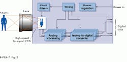
To build such a camera, Heuttig chose the HS0256J fast frame imager from EG&G Reticon (Sunnyvale, CA). Unlike the Kodak sensor chosen by Wintress, the EG&G device is a split-frame storage device with 16-µm square pixels. The split storage allows image data to be transferred to storage regions at the top and bottom of the CCD. Four taps on the device allow image data to be read out at 20 MHz per tap (see Fig. 2). This results in an 80-MHz data rate.
In building a camera around the HS0256J, Heuttig faced the same problems as Krialy at Wintress. "In essence," says Heuttig, "we are clocking four separate pieces of data from the sensor on four channels. Because the eye can discern even 1-2 least significant difference between the gain of these channels, we had to be very careful in the design of the analog processing section of the camera. Any difference between the channels would result in a crosshair across the image when it is displayed."
While the analog signal-conditioning circuitry remains proprietary, AOA uses two Analog Devices 9058 8-bit flash converters to digitize the signals once gain, offset, and clipping have been set. Because each 8-bit, 50-Msample/s ADC features two matched 50-Msample/s, 8-bit flash converters on a single chip, only two such devices are required to digitize the four channels of data from the analog processing circuitry. Once digitized, they are read off as 32-bit (8 bit/channel) output for input to a frame grabber or image processor. Like Wintress, AOA also provides a frame grabber based on a PC/AT computer that can be used with the camera. AOA`s KineView camera and frame grabber are now being sold by EG&G Reticon (Potrero, CA) as the MD4256 digital CCD camera and the SB4001 frame grabber.
Subsampling for speed
Faster speeds can be obtained by reading out only partial frames. The trade-off is that the resulting image has fewer pixels. Redlake Camera (Morgan Hill, CA) uses partial framing in its current product, the MotionScope 500, to provide frame rates as fast as 500 frames/s. Only a 128 ¥ 128 piece of the 336 ¥ 243 array in the Texas Instruments (Dallas, TX) 255 CCD array is used. Galen Collins, vice president of engineering, says, "These pixels are processed by digital-signal-processing techniques to obtain the apparent size of 512 ¥ 512 pixels."
The camera uses a resampling filter, more specifically a 2-D 17 tap by 17 tap FIR filter programmed to do 1:4 expansion of the picture in both dimensions. "Because the raw image sizes are small," says Collins, "a somewhat small memory can typically hold 2000 images."
The camera`s microprocessor has nonvolatile RAM that stores settings (including frame rate, play versus record, trigger parameters, and shutter speed) when the power is turned off. After the microprocessor sets the timing generator to the proper timing for the user`s request, operation begins. The microprocessor also takes in external trigger and synchronization signals. The timing generator produces all of the timing for the CCD array and the memories and A/D converters. Timing for electronic shuttering of the video is also provided. The timing generator is mostly implemented in an Altera EPF81188 PLD.
The clock-drivers block produces the voltages and levels required by the CCD imager for proper operation. The analog process block and the A/D converter produce a digital form of the video. Gamma correction is an option (controlled by a DIP switch) that is implemented by a look-up table. First-in-first-out modules and data-path multiplexing provide for the proper flow of data to and from the large DRAM memory. The current model converts digital images stored in DRAM to an NTSC analog signal for display, but models due out later this year will allow digital readout directly from the DRAM.
The choice of the TI 255 CCD, which was designed for low-cost imaging at broadcast frame rates, was influenced by Redlake`s desire to make a low-cost camera. Another result of this is the use of a single tap from the CCD. Collins says, "Multiple-tap CCDs require multiple-channel electronics circuits. The single-channel design requires far less circuitry than these multichannel designs, allowing for lower cost of production."
Pushing the speed limit
When you require very-fast, high-resolution color to be digitized, it helps to have your own fab. That`s because CCDs used in such systems may require sophisticated architectures with many taps. If you are lucky enough to be the Eastman Kodak Motion Analysis Systems Division (San Diego, CA), that`s no problem.
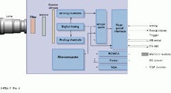
In the design of the company`s RO camera, which forms the basis of the Kodak EktaPro color motion analyzer, the company designed and developed a multiple-tap 512 ¥ 384 interline CCD sensor with antiblooming. Although much of the technical detail behind the camera design remains proprietary, the general design of the camera is similar to that of the Wintress and AOA cameras (see Fig. 3). After a number of taps are read from the image sensor, the signals are conditioned by preamps that set the gain, level, and offset of the signals. Before digitizing, a S/H is used to retain an average sample of the signal.
After conversion by an ADC, the resulting digital data are formatted and stored in image store memory. Up to 500 images can be stored on board the cameras. This image memory can then be transmitted under microcomputer control to a PCMCIA hard drive or flash memory module.
According to Kris Balch of Eastman Kodak, "The RO camera is designed to operate similarly to the film cameras currently being used in harsh environments." Prior to recording, the camera is set in a low-power mode. A signal is then sent to the camera over the RS-485 interface to ready the camera for recording. An additional trigger then triggers the camera recording until the image memory is full.
For those designers that do not own their own fab, PixelVision (Beaverton, OR) is offering a unique service that allows custom CCD devices to be built without incurring typical fab costs. Recognizing that many imaging requirements cannot be met with off-the-shelf CCDs, PixelVision`s Sandbox CCD foundry and design service allows several companies to produce CCD devices in "batch mode" at a cost of around $30,000, according to PixelVision`s Jim Janescek. With such developments, camera manufacturers and their customers may discover that finding a perfect match between camera and application becomes a lot easier.
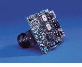
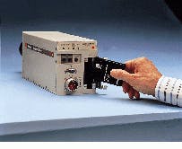
FIGURE 1. Wintress Engineering OPSIS 5000L high-speed camera is capable of capturing 648 ¥ 484 images at 60 frames/s. The camera uses an Eastman Kodak dual-readout KAI-0310 imager that is controlled by a field-programmable gate array from Altera. Output from the camera is an isolated 330-Mbit/s HOTLink serial interface that allows the camera to be placed up to 300 ft from a frame grabber or image processor.
FIGURE 2. Capable of digitizing 256 ¥ 256-resolution images at 1000 frames/s, the Adaptive Optics Associates KineView High Speed Video camera uses the EG&G HS0256J fast framing imager that outputs four taps at 20 MHz. Offset, gain, and clipping are then set before the signals are digitized by two dual 9058 analog-to- digital converters from
Analog Devices.
FIGURE 3. Eastman Kodak`s EktaPro RO imager has a proprietary 512 ¥ 348 color CCD
imager, which makes the camera capable of capturing 512 ¥ 348 color images as fast as
1000 frames/s and storing the images to disk or flash PCMCIA memory .
Looking at CCD specifications
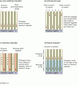
There are a variety of architectures used for moving charges from the CCD pixel site to the readout register, and a variety of these designs can be combined. The simplest dssign moves the charge from one pixel in a column to the next until they arrive, in series, at the readout register. Each row is received in this register at one time, and the charge is transferred horizontally off the chip. This line-address transfer method is simple, but, if the CCD receives more light during readout time, the image may appear saturated. This is known as blooming. To overcome this effect many CCD manufacturers are using antiblooming structures in their devices. These allow excess charge in the photosites to be dissipated, overcoming any blooming effects.
A variation on this type of CCD first reads out all the odd columns, then all the even columns. Although such interlace-scan CCDs offer faster readout than progressive-scan designs, such designs may not find great use in high-speed image cameras because captured odd and even images may be different, effectively lowering the resolution of the device.
A method that allows faster acquisition without using interlacing is interline transfer. Here, each column is equipped with a vertical shift register--a second column of capacitors masked from the incoming light. Pixel sites capture electrons, then shift the charges to the vertical shift register. The charges are then transferred to the readout register via masked capacitors while the pixels are gathering charges from another image. This approach allows the CCD to obtain images at a faster rate. But much of the area of the CCD chip may be used by the masked capacitors, limiting the resolution of the chip.
Frame-transfer or block-transfer is slower than interline transfer but is attractive because it offers higher resolution. Here, the charges from photosensitive capacitors are transferred off the array, but instead of entering a readout register, they are transferred onto a masked array that is the same size as the pixel array. Once the image is clocked off the pixel array, a second image can be obtained while the first image is being read from the masked array to the readout register below it
Different CCD architectures move the charge off the active pixels in different ways. In line-address transfer CCDs, charges move down the column of pixels to the readout register. This is also a progressive-scan (as opposed to an interlace-scan) CCD (a). Interlace-scan CCDs work much the same way as line-address transfer CCDs except that first odd columns are read out, then even columns (b). Interline transfer CCDs move charges from the pixels into vertical shift registers, which then move charges to the readout register (c). Frame-transfer CCDs move charges down the column of pixels onto a storage array (d)
