Researchers explore vision stimulator for restoring eyesight
Researchers explore vision stimulator for restoring eyesight
John Haystead
Contributing Editor
Researchers in the department of electrical and computer engineering at North Carolina State University (NCSU; Raleigh, NC), together with the Wilmer Eye Institute of John Hopkins University (Baltimore, MD), have developed the first elements of a prosthetic retinal-implant device aimed at restoring vision to patients afflicted with retinitis pigmentosa. One in 4000 Americans has this degenerative eye disease, where the photoreceptor cells of the retina fail to respond to light.
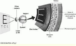
Earlier this year, the team completed work on a prototype wireless power and data receiver and neural stimulator. Bypassing the nonfunctional photoreceptor cells in the retina, this implantable stimulator works by providing direct electrical stimulation to retinal neurons (see Fig. 1). The 4.6 x 4.7-mm device is fabricated in 1.2-μm complementary metal-oxide semiconductor (CMOS) technology and drives a 10 x 10 array of retinal electrodes at real-time visual rates.
Data transmission
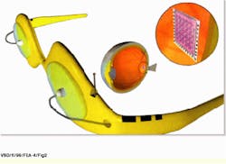
The complete retinal-prosthesis system is partitioned into two components: the neural stimulator chip to be surgically implanted inside the eye and a camera and transmitter worn externally on a pair of eyeglasses or goggles (see Fig. 2). The first system-design challenge was to find a way to bring power and data to the stimulator subsystem inside the eye.
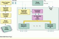
As described by Wentai Liu, associate professor of electrical engineering at NCSU, "We could have used a wired system, but such an invasive approach would be susceptible to infection, and the wire could also be broken during periods of rapid eye movement." Instead, a wireless RF power and data-transmission link was chosen that uses an inductively driven coil functioning as the transmitter and receive antenna (see Fig. 3). In the stimulator chip, the sine wave of the carrier signal is fed into a four-way bridge rectifier and low-pass filter to generate dc voltage.
Serial image data are transferred using a two-stage modulation scheme. The data are first converted into a pulsewidth-modulated (PWM) waveform, which is then used to amplitude shift key (ASK), or digitize, the carrier frequency. The present system operates at a carrier frequency of 2 MHz and a PWM frequency of 24 to 200 kHz.
The rising edge of the PWM waveform is the clock signal, whereas the duty-cycle transition is used to encode each data bit through an alternate-mark, modulation-inversion scheme. Says Liu, "This technique maintains an average power level with little data dependence and also allows the use of a simple, area-efficient demodulator circuit."
Although a laser-based transmission system was also considered, as described by Chris DeMarco, a doctoral student on Liu`s team, the problem was that "while the laser could deliver megabit-per-second video rates, it couldn`t deliver as much power as the inductively based system. Right now, our data rate is so low that the coil-based inductive system can handle it." Still, DeMarco notes that as the implant`s spacial resolution grows in size, the required data rate will also have to increase. "In the future, we may be looking at a hybrid system with an inductive system for power and an optical system for data," he adds.
Data decoding
During system operation, the encoded PWM waveform is recovered from the carrier wave by passing it through rectifying and low-pass filter circuits in the driver chip`s ASK demodulator. Amplitude shifts are detected using a comparator circuit that incorporates a 10-pF capacitor. A delay-locked-loop circuit with an integrated 200-pF loop-filter capacitor then recovers the clock and data from the PWM waveform.
The retinal neurons are stimulated using a bipolar current-pulse waveform. As described by Liu, the optimum pulse amplitude, timing, and duration are not always known because they depend on the patient`s degree of blindness. "Sometimes a higher current and a longer pulse are needed, whereas in other cases, a higher frequency is optimum," he says. The system is therefore designed to accommodate a range of blindness parameters.
The typical impedance of the implanted electrodes is 10 k, and the prototype implanted device can produce up to 600-μA current pulses with a 4-bit amplitude resolution, up to 500 image frames/s, and a pulse-timing resolution of 1/400 of the frame period.
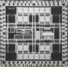
The driver chip contains 20 pulse-stimulator circuits (see Fig. 4). Each circuit implements 4-bit amplitude control, and all circuits operate in one of three preselected current ranges (200-, 400-, and 600-μA full-scale values and least-significant-bit increments of 12.5, 25, and 37.5 μA). Each stimulator is connected to five electrodes through a demultiplexer circuit.
Although the maximum 600-μA current provides the highest brightness level, Liu points out that the design goal was to generate gray-scale viewing. To accomplish this, the four data bits are used to divide the total current into 16 levels. The gray-scale images are generated by managing 15 parallel current sources and by switching 8, 4, 2, and 1 current sources during each frame either to the bias voltage or to ground.
External design
Whereas the internal driver-chip design has been completed, work is continuing on the design of the prototype external component. A miniaturized video camera and processing board have already been successfully tested with the driver chip. Design work is now focused on integrating the other components.
The original camera is an Omnivision Technology (Sunnyvale, CA) NTSC-type monochrome unit measuring 1 x 1 x 0.5-in. with a 320 x 240-pixel resolution at 30 Hz. This device will soon be replaced, however, with a new digital camera from COMedia (Hong Kong) that incorporates the Omnivision OV5017 0.25-in. CMOS sensor with a 384 x 288-pixel array. In preparation for future use in a possible medical unit, the research team is also designing its own CMOS-chip camera that will integrate a 64 x 64-pixel array and image-processing circuits in a single device.
The researchers are already using elements of the external system to test the interface to the internal component and analyze the image-data-to-waveform conversion process. The custom-designed 2.5 x 4-in. processing board incorporates an Altera (San Jose, CA) 100-k gate-programmable-logic device and 3 Mbytes of Samsung Semiconductor (San Jose, CA) synchronous random-access memory arranged in six 512 k x 8-bit modules. Three of the modules serve as independent frame buffers; the others are used as an indexing buffer. The board also currently contains an 8-bit, 30-MHz analog-to-digital converter, but this device will be bypassed by the digital camera.
As explained by doctoral student DeMarco, the programmable logic device provides a reconfigurable alternative to software-based processing while avoiding the associated turn-around time and cost of a custom ASIC. "By describing the processing operations in Verilog or VHDL, the programmable logic device can be quickly configured and alterations easily accommodated," says DeMarco.
The programmable board can rotate images as well as select which and when individual pixels will activate. According to Liu, this approach has been found to be an important capability for a biological system, because an adjacent group of nerve cells (or ganglia) in the retina must be given enough time to discharge between firing. To address this concern, the system is programmed to sequentially activate the array electrons in a well-spaced pattern.
The complete test setup is hosted on a standard PC using the Linux operating system, says Liu, because it is easier to write device drivers. Currently, image data are analyzed using an oscilloscope. However, Liu says the next step will be to set up a directly driven LED panel to view the actual images produced by the total system.
A specific area of continuing work involves the RF-signal transmitter, which must provide the required amount of current and voltage. Because each electrode can take a maximum of 600 μA, the entire 10 x 10 array requires a total of 60,000 μA. At the same time, however, because eye tissue has approximately a 10-k-equivalent impedance, an approximately 6-V differential is produced across the tissue. As a result, to produce the optimum positive/negative polarity biphasic signal, the transmission system must deliver about 12 Vdc, in addition to the 60,000 μA, to the inductive coil of the internal component. Currently, a Class-E amplifier design performs this task and converts the digital data into a 2-MHz RF carrier signal of about 50 to 60 mW. This approach carries the signal the total required distance of 1 cm from eyeglass to eye.
Although the research team is looking at integrating the RF amplifier circuits into the single-chip camera/ processor, they are encountering additional design difficulties because of the large inductance values (in the microHenry range) required. As noted by Liu, "Given that this portion of the system is part of the external unit, it may be more practical to implement it as an additional discrete component."
Human testing
The NCSU/Wilmer Institute collaboration plans to begin human testing of the prosthetic device (see "Imaging technology sheds sight," p. 32). According to Liu, however, this will pose additional engineering challenges such as the need for the hermetic sealing of the internal component to isolate it from eye fluids. Meanwhile, the NCSU team is working to finish the complete system prototype. In addition to the image collection and processing elements, the team is also developing a suitable battery for the system. The design goal for a wasteline-worn battery pack is a time-between-charges of 24 to 48 hours.
Imaging technology sheds sight
At the Wilmer Eye Institute at Johns Hopkins University (Baltimore, MD) researchers are concentrating on the biocompatibility aspects of the retinal-prosthesis chip for various degrees of blindness in humans. As noted by Mark Humayun, biomedical engineer and assistant professor of ophthamology at the Institute, "retinal tissue is extremely thin (on the order of 0.3 mm), making it extremely difficult to attach something without causing damage." Thus far, however, animal research has been promising, with some devices in place for more than a year with no evidence of neuron damage. A design team of researchers is now in the process of testing the impact of long-term electrical stimulation and the associated generated heat on the retina.
Although the North Carolina State University (NCSU; Raleigh, NC) chip has not yet been implanted in a human subject, Humayun has been able to test the principle of the artificial retina on 15 human volunteers. "To date we have shown that by stimulating the retina using a controlled pattern of tiny electrical pulses, patients can identify geometric shapes such as boxes or letter forms." For example, one patient with retinitis pigmentosa, who has participated in three studies, has seen color and shapes and has correctly identified the letter H.
Humayun says the results of these early tests are the impetus behind the research push toward actual patient testing using an implanted device. "Although we could, alternatively, first work toward developing a more-complex stimulation device, the problem is that it takes 35 to 40 minutes for a patient who has been blind for many years to even begin to see an image. This is an extremely long and uncomfortable time to be in an operating room. Before we can really examine the capabilities and limitations of the technology, patients will need time to wear the implant and get accustomed to it."
In addition, Humayun points out that is not yet clear that larger, more-complex stimulation arrays will be necessary to provide significant vision to patients. For example, he notes that early researchers in cochlear implants for the deaf initially believed that tens of thousands of auditory nerve cells would need to be stimulated to provide useful hearing levels. In fact, single-digit electrode counts have allowed patients to understand telephone conversations. "The human brain is capable of taking a very coarse image and making sense out of it," says Humayun, "and some data have already shown that a pixel array as small as 25 x 25 may be able to give people good vision."
The NCSU will begin laboratory testing the retinal-implant chip within the next six months. Humayun says they expect to begin in-patient testing with a fully functional prototype system within the next two years.
FIGURE 1. Implantable retinal prosthesis provides direct electrical stimulation to retinal neurons in an approach similar to the way that cochlear implants have restored hearing to some deaf patients. A driver chip is placed on the inside surface of the retina, opposite the damaged rods and cones and in contact with the relay cells to the brain.
FIGURE 2. Artist`s concept of the complete retinal-prosthesis system shows the eyeglass-mounted, single-chip camera/processor now in development, the recently completed wireless power and data receiver, and the neural stimulator chip.
FIGURE 3. During retinal-prosthesis-system operation, serial image data from the camera and image processor are first converted into a pulsewidth-modulated (PWM) waveform, which is then used to amplitude shift-key (ASK), or digitize, the carrier frequency. The encoded PWM waveform is recovered from the carrier wave by passing it through rectifying and low-pass filter circuits in the ASK demodulator. A delay-locked-loop circuit recovers the clock and data from the PWM waveform. The 20 pulse-stimulator circuits are connected to the electrodes via a demultiplexer circuit.
FIGURE 4. Die photograph of the data receiver and neural stimulator chip shows the locations of the driver, amplitude shift-key (ASK) demodulator, delay-locked loop (DLL) and control logic, and loop filter.
Company Information
Altera Corp.
San Jose, CA 95134
(408) 544-7000
Fax: (408) 544-7755
Web: www.altera.com
COMedia Ltd.
Tsuen Wan, NT, Hong Kong
(852) 2498-6248
Fax: (852) 2414-3050
Web: is4.hk.super.net/~comedia
North Carolina State University
College of Engineering
Raleigh, NC 27695
(919) 515-2283
Web: www.engr.ncsu.edu
OmniVision Technologies Inc.
Sunnyvale, CA 94024
(408) 733-3030
Fax: (408) 733-3061
Web: www.ovt.com
Samsung Semiconductor
San Jose, CA 95134
(408) 544-4000
Fax: (408) 544-4934
Web: usa.samsungsemi.com
Wilmer Eye Institute
Johns Hopkins Hospital
Baltimore, MD 21287
(410) 955-5080
Web: www.wilmer.jhu.edu


