Auto-adaptive technology increases dynamic range of CMOS sensor
Andrew Wilson, Editor, [email protected]
Fill factors of less than 100% and dynamic ranges of around 60 dB are currently common in many CMOS sensor devices. Whereas lower-than 100% fill factors are the direct result of the lateral integration of photodetector and pixel electronics, dynamic range is a function of full-well capacity and read noise at each photosite. At the recent VISION 2002 show in Stuttgart, Germany, Silicon Vision (Boxdorf, Germany; www.siliconvision.de) announced a CMOS-based imager that it claims overcomes these limitations and boasts a nearly 100% fill factor and a "linear" signal-to-noise ratio of 120 dB.
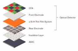
To achieve the nearly 100% fill factor, the company's locally auto-adaptive Lars III sensor uses an amorphous silicon (a-Si:H) detector deposited on an application-specific integrated circuit (ASIC). In the 766 ¥ 494-pixel Lars III imager, the optical detector consists of a rear electrode, a multilayer a-Si:H thin-film photosensitive device, and a transparent front electrode. The top layer of the optical detector is a thin transparent front electrode deposited as a continuous film. According to Jochen Braun, Silicon Vision vice president of sales and marketing, such vertically integrated thin-film-on-ASIC sensors achieve fill factors of nearly 100% and allow independent optimization of the detector and the ASIC process.
Developing a sensor with a dynamic range of 120 dB is accomplished using a locally auto-adaptive process. In this method, each photosite controls its integration duration automatically within the defined integration time set for the whole imager. As the photocurrent at each photosite is integrated to a voltage by an integrating capacitor, it is also compared to a fixed reference voltage at a fixed point in time. If a pixel exceeds this reference, integration is terminated to avoid saturation. If not, the integration time is doubled using a 12-step (or 60-dB) voltage ramp that ramps in a power of two series after every comparison is applied to all the pixels. Integrated capacity and the individual time-stamp value are captured as analog values in each pixel and read at the end of the full integration time.
Therefore, although each pixel site may exhibit a 60-dB linear intensity range, the absolute pixel intensity range is split between the absolute time information (60 dB) and the intensity information (60 dB) relative to the time information. By combining both signals on-chip, a "linear" dynamic range of 120 dB is achieved.
Silicon Vision demonstrated an imaging system based on the HDR-L30-CL camera from Deutsche Vaccuum Electronic GmbH (Woltersdorf, Germany; www.devael.de), one of the first cameras to integrate the Lars III sensor. Featuring a Camera Link interface, the HDR-L30-CL camera was shown in a windowing mode and digitizing a very high dynamic range image that included a highly illuminated fan rotating at 1800 rpm. Using this camera, no distortion and no background shining through the fan blades could be seen. Next to the fan, the company had positioned a black carton with black lettering. Using software to window through the 120-dB dynamic range of the image, lettering on the black carton could easily be seen.
According to Silicon Vision's Braun, the future of such amorphous silicon sensors looks bright. He says, "Scaling of CMOS sensors leads to a reduction of the spectral response, especially for long wavelengths. And for feature sizes less than 1 µm with a depletion depth of 1 µm, the quantum efficiency of a CMOS x-Si diode is already poor compared to an a-Si:H thin-film detector and dramatically decreases for still smaller feature sizes. This effect will be an obstacle in using future technologies for CMOS imagers, whereas it does not affect the thin film detectors of TFA/CMOS sensors," he adds.
Using an amorphous-silicon detector deposited on an ASIC, the Lars III imager consists of a rear electrode, a multilayer thin-film photosensitive device, and a transparent front electrode. A dynamic range of 120 dB is accomplished using a locally auto-adaptive process in which each photosite controls its integration duration automatically. As the photocurrent at each photosite is integrated, it is compared to a fixed reference voltage at a fixed point in time. If a pixel exceeds this reference, integration is terminated. If not, the integration time is doubled. Integrated capacity and individual time-stamp values are captured as analog values in each pixel and read at the end of the full integration time.

