SPOTLIGHT ON ADVANCED TECHNOLOGY: Vision and x-ray methods help semiconductor inspection find hidden defects
Manufacturers have integrated x-ray and optical inspection techniques to ensure product integrity and save test cost and time.
By Richard Amtower
Small, high-density semiconductor integrated-chip (IC) packages, such as ball-grid arrays (BGAs), have gained widespread developer acceptance because they enable increased device performance and printed-circuit-board (PCB) size reduction. But they also introduce acceptance inspection complications. Because the ICs in these packages have hidden solder joints, automated optical inspection (AOI) is no longer sufficient to ensure solder integrity. Accordingly, manufacturers have turned to x-ray inspection systems to check area-array and IC components.
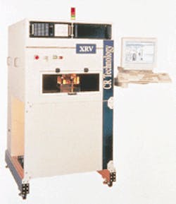
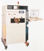
RIGHT. FIGURE 1. The CR Technology XRV Combo system uses its RTI-6520 vision inspection system as the underlying design platform, as well as an x-ray camera capability.
In fact, by combining AOI and x-ray imaging technologies, chip manufacturers, system assemblers, and developers can reap the benefits of both without sacrificing operational throughput or test time. The result is an integrated test system that cost-effectively inspects assembled PCBs.
Automated optical inspection systems were first introduced to PCB assembly in the early 1980s. Designed to replace human inspectors in checking PCBs for visible defects, such as missing parts, placement, and similar errors, these inspection systems were expensive, slow, and difficult to program. But improvements in computing power, software, and imaging technology have spawned a new generation of test systems that can be used at several points in the production process, either in-line or stand-alone. In a typical surface-mount scenario, board inspection is performed after parts placement, reflow soldering, and/or final assembly.
Essentially, AOI systems consist of one or more video cameras, lighting, and an image-processing computer. To compensate for the limited resolution of video cameras, these inspection systems use a combination of multiple cameras, indexing camera heads, and/or indexing PCB fixtures to check the entire surface of a PCB with high-resolution magnification. Typical defects found by AOI systems include missing parts, wrong components, polarization errors, part-placement errors, and solder defects. All defect information is identified and reported for analysis and rework.
The latest AOI systems are essential in PCB production because they perform fast, repeatable, and accurate inspections, find and identify defects before in-circuit or final testing, reduce production costs, and improve quality. But AOI systems can analyze only visible features. With the advent of BGAs, microBGAs, chip-scale packages (CSPs), flip chips, and other hidden-connection devices, component and board manufacturers are installing x-ray systems to analyze the critical solder joints of these new-generation packages.
RIGHT. FIGURE 2. Typical ball-grid-array (BGA) substrate is positioned for visual inspection as to correct part number, orientation, and solder balls. This substrate shows no apparent defects (left). X-ray inspection reveals the solder balls more clearly and therefore some hidden defects. These defects include the dark rectangles, which are solder bridges, as well as undersized solder balls near the center. They indicate poor or no solder reflow and an excessively large void, also at the center (right).
X-ray inspection of PCBs became practical with the introduction and development of real-time x-ray systems, which eliminated the cost and delays associated with film processing. A typical x-ray system is a cabinet-housed machine with lead-shielded walls and interlocked doors. It includes an x-ray source with enough power to penetrate the target PCB and provide sufficient resolution to image the expected range of defect sizes. An x-ray-sensitive video camera converts the x-ray of the PCB to a video signal, which is then enhanced and analyzed.
X-ray inspection is the best technology for identifying the shorts, voids, opens, misalignments, and solder integrity of area-array chip packages. Unfortunately, automated x-ray systems can require days or weeks of set-up time before they can inspect a PCB. Further, off-line systems do not accommodate 100% inspection and cannot verify the presence or absence of correct components, component orientation, polarization, or visual features.
Technology alliance
An integrated, combination x-ray/vision system offers major advantages over each separate technology. Incorporating both x-ray and vision inspection into one in-line machine yields systems that can provide complete analysis without compromising line speed. These combination systems enable manufacturers to inspect 100% of the hidden solder joints of BGAs, flip chips, and other CSPs. They are also able to simultaneously inspect for correct parts, positions, orientations, and other visual features, and can be set up to inspect a new PCB in less than one hour.
One such system, the CR Technology XRV Combo integrated x-ray/vision machine uses the company's RTI-6520 in-line AOI system as the underlying design platform (see Fig. 1). The XRV is a moving-source system in which the PCB undergoing test remains stationary while the x-ray cameras and x-ray tube move over it. An overhead x-y gantry carries two vision cameras and one x-ray camera (or detector) and the light source. The bottom stage is a rotary plus z stage. Rotary motion covers the x and y directions, and the z stage enables changes in magnification. This platform results in no speed impact on vision inspection and allows an x-ray machine to be built with a small footprint.
CR Technology built its own x-y camera gantry using Thomson CSF (Totowa, NJ) rails and lead screws to obtain some proprietary advantages and also developed its own white lighting and directed-LED lighting systems. White lighting is accomplished with the use of generic small incandescent bulbs, about 5 mm in diameter, to enhance solder inspection and achieve improved fiducial recognition.
The company drew on the expertise of several vendors to provide other elements of the XRV Combo. The conveyor system can accommodate as many as four CCD cameras to deliver visible images of an 18 x 20-in. PCB, but it is usually shipped with three cameras. The XC-75 vision cameras, which are RS-170 area-array units from Sony Electronics (Park Ridge, NJ), were chosen for their reliability, sensitivity, and availability.
The x-ray camera uses fluorescent screens that glow when illuminated by x-rays, converting the x-rays to visible light. These screens are available from a number of suppliers, including 3M, Fuji, Dupont, and Eastman Kodak. The company uses models from either 3M (St. Paul, MN) or Fuji Electronics America (Torrance, CA). An intensified camera to detect the converted visible images from Pulnix America (Sunnyvale, CA) uses an area-array microchannel plate to amplify the weak output of the fluorescent screens.
X-ray images are inherently weak and noisy and therefore require image enhancement. To do this, the XRV system uses a proprietary PC-compatible image-enhancement board based on a field-programmable logic array (FPGA) from Xilinx Inc. (San Jose, CA). This board, which acts as a frame grabber, performs image averaging and contrast enhancement and is integrated into an industrial-design PC built around a 650-MHz Pentium III from Intel Corp. (Santa Clara, CA).
System software
The XRV system software is an extension of the RTI-6520 software, which runs on Windows 98/NT. The development system uses Microsoft Visual C++ 6.0 and the Matrox Imaging Library (MIL) from Matrox Electronic Systems Ltd. (Dorval, Quebec, Canada); it occupies about 500,000 lines of C++ source code. Matrox tools were chosen based on speed, cost, and completeness of image-processing functions. The development system uses enhancement features such as contrast adjustment and image filters such as high pass, blob, histogram, and correlation.
The software user interface aids the technician in setting up and running the system. It is a graphical user interface developed with Visual C++ and uses calls to the MIL for image-processing and machine-vision functions. The user interface is application oriented and designed to facilitate PCB inspection for operators who have no machine-vision skills. It also has a computer-aided-design data interface in generic format to handle different inputs and merely needs to be set up part designator, x-y location, and rotation. This interface approach is intended to speed program creation and to provide functions such as statistical process control, data logging, and operator and board serial-number tracking.
Special algorithms for BGA inspection and x-ray solder inspection measure such defects as voids, shorts, and missing balls, and also allow the technician to adjust the pass/fail criteria. These algorithms measure each solder ball individually and support x-ray solder inspection for fast checking of various lead types. New inspection algorithms can be linked in the form of a dynamic link library to expand the inspection profile.
Hidden defects
A PanoView SVGA flat-panel monitor supplied by CTX Opto (Sunnyvale, CA) runs from the PC's monitor output port. It displays a video or x-ray image, a map of the board under test showing the proper location of components, and a window that shows the parts that have failed and all the parts in the component library for that board.
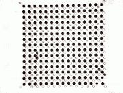
RIGHT. FIGURE 3. Visual inspection apparently shows no defects in the leads of this array. However, x-rays reveal a lead with insufficient solder in the heel of a gull-wing lead (light circle near center).
Most features on PCBs—including component presence or absence, correct component identification, position, orientation, and integrity of visible solder joints—are inspected using the XRV's video cameras, visual images, and machine-vision algorithms (see Fig. 2). At the same time, the x-ray subsystem verifies the integrity of hidden connections. Hidden defects usually occur at the solder-ball connections under BGA, microBGA, CSP, and flip-chip devices. In addition, solder joints in J-lead devices are difficult to detect for both human inspectors and AOI systems. On the common gull-wing-lead devices, only the fillet or outermost solder connection can be viewed; the more important heel area, hidden underneath the lead, is concealed from visual inspection (see Fig. 3).
Common BGA defects generally result from problems in manufacturing the solder balls prior to assembly and from problems in reflow-soldering the device to the PCB. Typical ball-manufacturing defects include missing, extra, and improperly positioned solder balls. Reflow soldering can produce voids, solder bridges, or insufficient solder problems. Only x-ray inspection can effectively detect these problems. Furthermore, x-ray inspection also monitors the quality process, providing the immediate feedback required for proactive process management.
When a board populated with area-array packages passes after being inspected for hidden defects, the shutters of the lead-shielded x-ray cabinet open. The board is then passed out along the conveyor, where it may be cycled to another system for additional assembly operations or passed to a handler for packing. For a failed board, the XRV generates a failure map, which is matched to the board's barcoded identification number and stored in a central file. Repairs can be performed by a technician accessing the failure map and board number at a rework station.
The need for this type of test system is just emerging as the experience of numerous manufacturers demonstrates that today's PCB production requires both AOI and x-ray inspection systems to ensure high product quality and reliability. But technology continues to improve; a related system is being developed with enhanced x-ray image quality and more analytical tools.
RICHARD AMTOWER is president and chief executive officer of CR Technology, Aliso Viejo, CA 92677.
Company Information
CTX Opto
Sunnyvale, CA 94089
(408) 541-6060
Fax: (408) 541-6068
Web: www.ctxopto.com
Fuji Electronics America
Torrance, CA 90503
(310) 214-5100
Fax: (310) 214-5105
Web: www.fuji-electronics.com
Intel Corp.
Santa Clara, CA 95052
(800) 548-4725
Web: www.intel.com
Matrox Electronic Systems
Dorval, Quebec, Canada H9P 2T4
(514) 685-2630
Fax: (514) 822-6273
Web: www.matrox.com/imaging
Pulnix America
Sunnyvale, CA 94089
(408) 747-0300
Fax: (408) 747-0880
Web: www.pulnix.com
Sony Electronics
Park Ridge, NJ 07656
(800) 686-7669
Web: www.sony.com/professional
Thompson CSF
Totowa, NJ 07512
(973) 812-9000
Fax: (973) 812-4191
Web: www.tes.thomson-csf.com
3M
Austin, TX 78726
(800) 328-1371
Fax: (512) 984-7279
Web: www.3m.com
Xilinx
San Jose, CA 95120
(408) 559-7778
Fax: (408) 559-7114
Web: www.xilinx.com


