SEMICONDUCTOR INSPECTION: Wafer inspection system reduces scrap by up to 7 times
Insemiconductor wafer manufacturing, lithographic processing techniques result in layers of oxide, polysilicon, or metal that may be unevenly deposited across the surface of the wafer. Before further lithographic processing can occur, chemical mechanical polishing (CMP) is used to planarize these layers. A polishing head is rotated across the wafer to even out the irregular wafer surface. After each polishing step, the wafer must be examined to ensure that no residual material remains on the wafer surface.
"In the past," says Romik Chatterjee, vice president of business development atGraftek Imaging, "this process was performed manually -- a process that was subject both to operator error and wafer breakage."
For these reasons, Spansion (www.spansion.com), a flash memory designer and manufacturer, commissioned Graftek to develop a machine-vision system that automatically detects residual metal film on patterned, metalized wafer surfaces.
The system was required to detect these defects across multiple wafer types using only the acquired images to determine the number and types of defects present without any prior knowledge of the die pattern on the wafer.
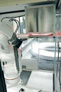
For the Residue Detection System (RDS), a six-axis robot fromYaskawa Motoman Robotics was used to pick the wafer from the CMP tool and place it within a custom 12 × 12 × 12-in. enclosure (see figure).
"Due to specular reflection of the wafer material, a uniform diffuse light distribution was required across the field of view," notes Chatterjee. Unfortunately, a dome or cloudy day illuminator (CDI) could not be used for this purpose because such a CDI/camera combination results in uneven illumination at the center of the camera's field of view.
Rather than adopt this approach, Graftek used a red LED source coupled to a custom-built diffuser to illuminate the wafer. Then images are taken of the surface of the wafer using a 1600 × 1200 × 12-bit monochrome FireWire camera fromAllied Vision Technologies (AVT). Fitted with a wide-angle lens, this camera is capable of viewing the entire 200-mm wafer from a distance of 150 mm.
After images are transferred to a host PC, the wafer orientation is determined by thresholding the image and determining the position of the notch on the wafer using IMAQ Vision software fromNational Instruments (NI). Once the orientation of the wafer is known, the position of any residual metal on the film can be accurately plotted.
"In many semiconductor inspection applications developed to detect defects," says Chatterjee, "different recipes are required to inspect the wafers for each product type and stage of the production process." However, with the RDS system this is not the case. Instead, custom pattern-recognition software written in C and incorporated into LabVIEW is used to detect specific patterns and textures on each wafer surface. Any deviations from the detected texture are then identified as defects by applying an algorithm similar to that of adaptive filtering.
"By tuning the size of detected defects with a large dataset of 20,000 wafers, false failures are minimized while known failures are detected," says Chatterjee.
After inspection, the robot moves the wafer from the inspection station to the next processing stage using an NI PCI-6520 industrial I/O board embedded in the PC. This sends 24-V signals to the polishing tool that in turn controls the motion of the robot.
According to David Lorek, an equipment engineer with Spansion, the RDS has resulted in wafer break jeopardy being reduced by 95% and between 3-7 times reduction in scrap wafers or wafers that need to be reworked.

