Optical processing systems ENABLE PATTERN RECOGNITION
Optical processing systems ENABLE PATTERN RECOGNITION
By Barry Phillips, Contributing Editor
Digital vision systems can be overtaxed by the intense number of computations required in real-time pattern recognition. Often, multiple CPUs must be used in parallel. These high-speed digital electronic systems can be prohibitively expensive. But with the advent of high-resolution, high-frame-rate, electronically addressable spatial light modulators (SLMs), hybrid optoelectronic vision systems can outpace their digital counterparts in pattern-recognition applications.
By early 1997, 512 ¥ 512 resolution, 1-kHz-frame-rate SLMs will become available. "Our upcoming analog 512 ¥ 512 SLM operates at 8.4 Gbit/s," notes Steve Serati, cofounder of Boulder Nonlinear Systems (Boulder, CO). "You could put enough digital hardware together to match this, but it`s exceedingly expensive to build a system that will run this fast," he says.
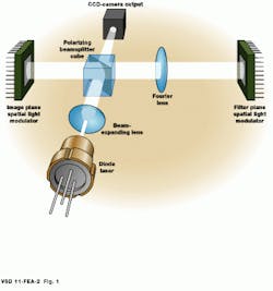
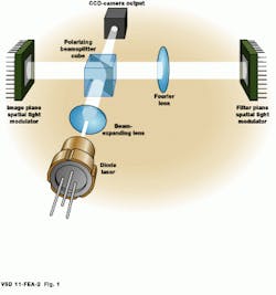
At the heart of every optical correlator is a spatial light modulator (see Fig. 1). Like liquid-crystal displays (LCDs), SLMs are electrically addressable--they can display an image or pattern. To find specific features in an image, the image is first written electronically to an input SLM. This image is reflected with a laser and passed though an optical lens, which produces a two-dimensional (2-D) Fourier transform of the image. The resulting image is then directed onto a second SLM, called the filter SLM, that has been electrically programmed with a Fourier transform of the pattern of interest in the input plane.
The resultant image then travels through another lens, which performs a second Fourier transform. The output is equivalent to the 2-D correlation of the input image with the filter plane. If the filter pattern corresponds to features that exist in the input, it results in a bright spot in the output image at the location of the pattern in the input scene. This location is typically captured by an imager or CCD at the output. Because filter SLMs can be rapidly updated with thousands of precomputed filter templates, objects that may be in any one of a thousand possible orientations can be rapidly found in complex images.
Commercial SLMs
Although optical correlators have been in development for years, they have failed commercially due to the lack of suitable SLMs. Early attempts to commercialize optical processors that used SLMs adopted from large LCDs resulted in systems that were hard to keep thermally stable. With the advent of SLM microdisplays with enough resolution to handle complex images, optical processors are moving from the optics table into industrial inspection systems.
Like LCDs, SLMs can be manufactured as both binary and analog devices. In binary devices, each pixel in the device is either switched on or off. Analog, or gray-scale devices, on the other hand, can display several levels of gray. With binary SLMs, ideal (analog) filter algorithms must be approximated as binary functions. Because they can display continuous functions, analog SLMs allow developers to build more efficient filtering systems.
Using ferroelectric liquid crystal on single-crystal silicon technology, Boulder Nonlinear Systems has developed both 128 ¥ 128 analog (gray-scale) SLMs and 256 ¥ 256 binary SLMs (see Fig. 2). Both devices operate at frame rates up to 10 kHz, enabling an optical correlator to perform up to 10,000 optical-filter operations per second. The company`s 512-resolution device is expected late next February.
Displaytech (Boulder, CO) also offers a 256 ¥ 256 binary reflective device. The device is constructed using traditional CMOS to create more compact devices with higher resolutions.
Recognizing patterns
By coupling SLMs to optical systems, identification systems that correlate images against stored patterns can be built cost-effectively. Emerging applications for optical correlators include agricultural inspection, face recognition, and medical image screening.
Boulder Nonlinear Systems is already working on an optical correlator for the inspection of produce such as apples. To accomplish this, the company uses an electronically switchable liquid-crystal tunable filter--a transparent optical device that, when placed in front of a CCD camera, can select the frequency of imagery that is brought into the correlator. For any given frame, the frequency of the tunable filter can be switched, and patterns that are known to exist at that frequency can be observed. The filter can be switched between different wavelengths in the visible and near-infrared ranges within 40 µs.
Optical correlators are useful in medical imaging systems. Using a 256 ¥ 256 binary SLM, the University of Colorado (Boulder) has developed a optoelectronic system that can accelerate morphological feature detection to speed the screening of Pap-smear slides (see "Optoelectronics speeds Pap-smear analysis" below).
At Lockheed Martin`s Advanced Processing Group (Denver, CO), an 80-GFLOP optical correlator based on 256 ¥ 256 binary ferroelectric technology is being used for histogram analysis/manipulation, contrast/edge enhancement, fast Fourier transforms (FFTs), and spatial filtering operations. "Our processing systems are suited for the FFT and related spatial-filtering operations such as correlations and convolutions," says Bill Hahn, senior engineer at Lockheed Martin. Currently, the company is using the part with neural networks to accelerate mammogram-screening tasks such as identifying cancerous lesions in x-ray data.
Essex Corporation (Columbia, MD) is taking lessons learned from military image processing and applying them to medical imaging. The company`s ImSyn optoelectronic processor is a 2-D Fourier-transform processor that is capable of real-time 256 ¥ 256-point transforms. According to Essex spokesman David Parry, "We are in the validation stage of an MRI application with the University of Maryland and have demonstrated 256 ¥ 256 Fourier transforms at 20-40 frames per second."
Optically addressable SLMs
Even as commercial SLM systems that can scan thousands of patterns per second enter the market, researchers are moving ahead with a new generation of optically addressable SLMs that are capable of running in the hundreds of kilohertz range. Using GaAs technology to manufacture SLMs, Sanders, a Lockheed Martin company based in Nashua, NH, has created prototypes of binary 128 ¥ 128 SLMs that operate at 390-kHz frame rates and 256 ¥ 256 devices that operate at half that rate.
The use of electro/photorefractive materials such as quantum wells may revolutionize optical processing. With its smart pixel array, researchers at the University of Southern California are using quantum-well diodes and GaAs field-effect transistors to accelerate morphological image processing (see "Optical computer uses per pixel processing to push performance," p. 32).
But while such spatial light modulators represent a magnitude improvement in speed, tough system-integration issues lie ahead. Even with today`s correlators, data rates from SLMs are faster than the digital circuits needed to transfer data to and from them. Although GaAs circuits can be used for this function, their cost may make such systems prohibitively expensive in all but military applications.
FIGURE 1. To rapidly recognize features within images, optical correlators use spatial light modulators and Fourier optics. By correlating the Fourier transform of the image with the transform of a feature, optical correlators can operate far faster than their digital counterparts.
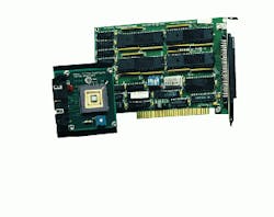
FIGURE 2. Lockheed Martin`s 80-GFLOP optical correlator is based on 256 x 256 binary ferroelectric technology. By using the part with neural-network software, the company has accelerated mammogramscreening tasks such as identifying cancerous lesions in x-ray data.
Optoelectronics speeds Pap-smear analysis
Women from 20 to 64 years old are encouraged to have a cervical cancer screening every year. Pap-smear slides are prepared from cellular samples obtained from the cervix. All such slides are sent to a cytology laboratory for staining. There, a cytologist examines each slide-typically for 10-15 mins--under a microscope and determines if the slide is normal or abnormal. Each smear can contain up to 100,000 cells.
Because this is tedious and repetitive, it results in a false negative rate (incorrect diagnosis of a slide displaying abnormal cells) in excess of 17%. Automated cervical-smear examination is therefore desirable as a quality-control mechanism for detecting abnormal cells missed by human inspection and as a primary diagnostic cytology screen.
In automated cervical-smear screening, features of interest are hidden in a vast search area. Suspicious cells are identified on the basis of their enlarged nuclei. A normal cell`s nuclear diameter is between 6 and 8 µm, while a suspicious cell`s nuclear diameter ranges between 10 and 22 µm. To detect this difference in size, the slide is sampled at a resolution of 1 µm/sample.
A typical Pap smear has a cover glass area of 50 ¥ 25 mm, which translates to processing more than a billion pixels for every slide. Acquiring and processing these data in approximately five minutes is difficult and expensive, even with high-speed electronic systems. At the University of Colorado (Boulder), an optoelectronic system has been built as the front end of a two-part automated screening system. In operation, the slide is first examined at 1000 frames/s to identify and retain suspicious regions and eliminate normal regions from further processing. This operation is called region-of-interest (ROI) detection and reduces the amount of data that must be processed by 1000:1.
ROI detection is performed using a morphology feature detector called the hit/miss transform (HMT). The HMT detects the shape/size of the cell nucleus. If the nucleus is circular with a diameter larger that 10 µm, the cell is identified as suspicious. An optoelectronic implementation of the HMT using two 256 ¥ 256 ferroelectric-liquid-crystal SLMs detects ROIs that can be further processed by ROI classification algorithms.
-- Ramkumar Narayanswamy, Rosemary J. Stewart,
John L. Metz, and Kristina M. Johnson
Optoelectronic Computing Systems Center
University of Colorado
Boulder, CO 80309-0525
(a) Pap-smear image displaying abnormal and normal cells from the cervix and (b) the result of the HMT operation to detect ROI simulated on a digital computer superimposed on the original image.
Optical computer uses per-pixel processing to push performance
Single-instruction multiple-data architectures (SIMDs) used in vision and image processors contain arrays of simple processing elements that compute images on a per-pixel basis. But, despite their inherent speed, feeding large amounts of image data to such processing engines causes I/O bottlenecks. To overcome these bottlenecks, a two-dimensional parallel SIMD pipeline has been developed at the University of Southern California.
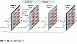
In operation, two-dimensional (2-D) frames of digital data are moved optically between pixel arrays, dubbed smart pixel array cellular logic (SPARCL). These pixels are processors that perform digital operations on incoming data frames and/or data frames stored within the pixel array.
In the optical system, data are moved between integrated circuits to create a 2-D parallel-pipeline system. The first chip formats an optical frame of data. Once the frame is composed, it is transferred optically in a single clock cycle to the next chip, which performs logic operations on the frames and passes them onto the final device. This converts optical data back to electrical signals.
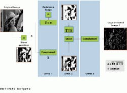
Such pipeline architectures allow the intermediate devices to perform logic operations and data format conversion simultaneously. Two-dimensional image data enter the processing as optical signals. Each chip contains an array of pixels that perform operations based on binary image algebra. This image algebra decomposes complex data-manipulation algorithms into complement (logical NOT), union (logical OR), and dilation operations. Complement and union functions operate on bit values stored within the pixel`s three-bit memory. Dilation functions are performed by ORing together one or more bits stored in its four neighboring pixels. Data enter and exit these elements either from neighboring pixels or optically.
To perform edge detection, a block quantizer splits the original image into small data frames to match the size of the pixel arrays. Each of these frames is then operated on by a dilation with a reference image, two complements, and a union. These four commands require only three clock cycles on-chip to perform an edge detection. This is a huge reduction compared to the number of clock cycles required in a serial processor.
-- C. B. Kuznia, Jen-Ming Wu, Chih-Hao Chen, Bogdan Hoanca, and A. A. Sawchuk
Signal and Image Processing Institute
University of Southern California
Los Angeles, CA 90089-2564
Multiple pipelined optical processors contructed as a single-instruction multiple-data processor are being used to speed image processing at the University of Southern California. While, the first IC provides electrical to optical conversion, intermediate devices perform logic operations on optical data frames. Finally, optical data are converted back to electrical form.
By using parallel-processing techniques, operations such as edge detection can be performed in three clock cycles. After block quantization, the complement of the image is dilated with a reference image. The union of the resultant image with complement of the original image detects the edges in the image. This can be seen visually by displaying the complement of this union.
