Smart cameras boost CCD performance
Andrew Wilson, Editor, [email protected]
In developing solid-state cameras for machine-vision systems, camera designers must overcome many of the physical limitations of the CCDs themselves. These include the nonuniform quantum efficiency (QE) in both horizontal and vertical directions across the imaging array, blooming, and Bayer color aliasing effects. “By compensating for such effects within the camera,” says Dave Krekelberg of illunis (Minnetonka, MN, USA; www.illunis.com), “captured images can more accurately represent the scene being imaged.”
Illunis designed its XMV cameras with specialized circuits that analyze and correct the unwanted effects of CCD imagers. The circuits use the concept of a detector, which is a circuit that measures image data within an image window. Information gathered by the detectors can determine if the image is suitable for the end user. These circuits operate on the full image bit depth and at the pixel rate of the camera, so no additional postprocessing is required.
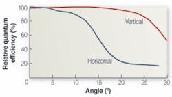
In the design of its KAI-11000 11-Mpixel image sensor, for example, Kodak Image Sensors (Rochester, NY, USA; www.kodak.com/go/imagers) uses 9-µm-square pixels with microlenses to increase the QE of the device at each pixel site. These microlenses direct light toward the photogates of the imager to increase the QE of the device. “In doing so,” says Krekelberg, “the QE of the sensor will be directly related to the angle of light entering the pixel. Due to the design of the sensor pixel, this angle dependency is much greater in the horizontal direction than the vertical direction” (see figure). Because of this dependency, illunis designed a microlens vignetting circuit (MVC) to apply a gain correction to each pixel in each column of pixels in the sensor, based on a look-up table (LUT).
In the KAI-11000 sensor, Kodak uses microlenses to increase the QE of the device. Because the QE of the sensor is directly related to the angle of light entering the pixel, a gain correction must be applied to each pixel based on a look-up table.
“Because the MVC LUT has an entry for each pixel in a column, a greater gain can be applied at the two ends of the line to correct for the QE drop from the light angle to the microlens pixel,” he says. By incorporating this circuitry into its XMV camera line, illunis allows the system integrator to optimize the output of each image to compensate for these effects.
“Often,” says Krekelberg, “cameras based on such devices capture images where an intense spot of light is present. This results in the charge capacity of the vertical CCD being exceeded-a charge that then spills vertically into the image area as well as the optically shielded area of the CCD. Because a severely bloomed image will feature a streak of saturated pixels that extend into the optically shielded (black) region,” says Krekelberg, “a blooming-detector circuit can be used to measure the number of pixels in a window/area that is oversaturated.”
In the XMV-11000, for example, the maximum size of the blooming detector is 4096 x 16 lines, which is the width of the imager and the number of dark rows. To measure the number of pixels that are oversaturated, illunis’ blooming detector uses a window defined by a start line, a size, and the horizontal limits of the device’s autoexposure window (AEW). To check whether blooming may have occurred, the brightness of the image within the auto-exposure window must first be determined. This is done using an exposure histogram detector that measures the number of pixels at specific brightness levels.
To count the number of pixels within the AEW, several bins are defined for black measurement (BIN0), mid-range (BIN1 and 2), bright points (BIN3), and saturated pixels (BIN4). To detect whether an image is bloomed, the number of pixels with specific values within the blooming detector window are compared with the BIN3 and BIN4 values obtained from the histogram of the autoexposure. If the number of pixels falls within these limits, then the detector is incremented. If the count falls outside these limits, then the image may have a blooming defect.
“This blooming feature is especially important in aerial applications,” says Krekelberg, “where an image that is bloomed can be retaken with an alternative exposure.” By implementing such functions into its XVM camera line, developers of aerial reconnaissance systems can ensure a first-pass success when capturing imaging data.
“Where color imaging is important,” says Krekelberg, “the use of the Bayer filter can also pose problems. In Bayer-based color imagers, pixels on the image sensor are covered with a mosaic of RGB transmissive filters. This raw Bayer data must be converted to RGB data using interpolation methods, including nearest-neighbor replication, bilinear interpolation, and smooth-hue transition interpolation (seeVision Systems Design, Sept. 2004, p. D11).
“While such techniques produce color images,” says Krekelberg, “the incomplete sampling in the image plane and the phase offsets of the color channels lead to aliasing effects.” To overcome this effect in its XMV-11000 camera, illunis has contracted with a third-party vendor to develop an optical blur or antialiasing filter with a 9-μm pitch to reduce the color-aliasing artifacts caused by spatial phase differences among the color channels. “While these blur filters reduce the need to reduce color aliasing at the expense of image sharpness,” says Krekelberg, “they produce extremely high quality images.”

