CMOS imagers fit niche vision needs
Improvements in CMOS technology have increased flexibility and decreased costs in high-speed or low-light applications.
By R. Winn Hardin, Contributing Editor
For the past decade, the machine-vision industry has waited for complementary-metal-oxide-semiconductor (CMOS) cameras to eclipse the more popular and expensive charge-coupled-device (CCD) cameras. CMOS cameras can be made less expensively because the manufacturing processes are similar to those used for making microchips; this similarity means that logic circuits and memory can be added to the same wafer containing the sensor chip, including A/D electronics. When A/D conversion on the camera is integrated on the camera, the need to buy frame grabbers for many imaging systems may be eliminated.
Unfortunately, efforts to optimize logic-based CMOS manufacturing for imaging sensors has proven more difficult than expected. CMOS sensors suffer from nonuniformity, because each pixel has its own charge-to-voltage conversion, while a CCD sensor uses a single charge-to-voltage conversion for every pixel. This fact, however, allows the CMOS sensor to be selectively read ("windowing"), so that the user can configure the sensor to read out only certain rows and/or columns of pixels, increasing the frame rate of the sensor by effectively reducing its size. Windowing is the biggest benefit of CMOS technology.
When camera designs containing programmable "full descriptors" are added to a CMOS sensor, the size of these windows, along with other performance characteristics such as gain and exposure time, can be changed from frame to frame, giving the user maximum control of the sensor and leading to small-form-factor, highly configurable, high-speed CMOS camera designs. For example, in applications with objects of different sizes—such as PCB inspection where passive components are very small and a microchip is relatively large—windowing can significantly speed up average throughput.
CONFIGURABLE SYSTEMS
"We used CCDs in the past, but then we switched to a CMOS camera with FireWire interface," explains Pierre Aubrey, executive vice president of ShapeGrabber, a supplier of imaging/scanning systems that use a laser and CMOS sensor to create 3-D maps of objects. "In addition to a high-speed consumer-based interface, CMOS gives us a fair bit of control over things such as windowing and exposure. We also benefit from a price point of view." According to Joel Bisson, president and CEO of PixeLink, a megapixel CMOS machine-vision camera can cost $1800, while a similar CCD camera could cost $3000.
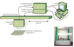
According to ShapeGrabber application engineer Nicolas Marmet, ShapeGrabber uses the 10-bit, 1280 × 1024-pixel PixeLink PL-A653 CMOS OEM Imaging Module with 12.7 frames/s at full resolution and a rolling shutter in its Cyclone AI810 multiaxis scanning system. The Cyclone is a 3-D scanning system that includes a laser line projector and CMOS camera positioned at fixed angles on a moving horizontal rail. A vertical rail allows the operator to move the laser/camera up or down to accommodate larger parts, and a rotating stage allows the total system to scan five of the six sides of an object without operator intervention. The laser line scans across the object, and the CMOS camera captures changes in the line's shape (see Fig. 1).
Image-processing software running on a PC converts the distortions in the laser line to 3-D coordinates through triangulation algorithms that use the known positions of the laser line projector and the CMOS camera relative to the object under inspection. High-speed FireWire interfaces with up to 400 Mbytes of bandwidth and dual-processor PCs boost the system's throughput.
The ShapeGrabber 3-D scanner moves the laser line in increments as small as 20 µm. Even with dual-processor PCs, acquiring that much information can slow the machine to rates of 14 frames/s using a megapixel CMOS camera. By windowing the sensor to the same size as the laser line, it can reduce the data set for analysis and improve the system's throughput by a factor of four or greater.
Marmet adds that although CCD sensors can be windowed to reduce the amount of transmitted data, the sensor typically still reads out the entire array, limiting increases in frame rates related specifically to the camera. "It's not impossible to get this with CCD imagers, but the features are not there naturally all the time," Marmet concludes.
HIGH-SPEED CAPTURE
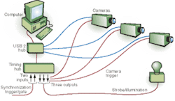
By combining CMOS sensors with gigabytes of local memory, Integrated Design Tools (IDT) fully realizes the speed of CMOS sensors for applications such as particle image velocimetry, fluid flow analysis, high-speed impact analysis, and high-speed inspection. The IDT X-Stream line of cameras, timing hub/pulse generators, and data-acquisition hardware allow the CMOS sensor to acquire image data at up to 5145 frames/s for a 512 × 512-pixel array to 250 frames/s for a 2300 × 1700-pixel array (see Fig. 2).
"As we make the regions of interest smaller, the frame rate goes up accordingly," explains Luiz Lourenco, IDT CEO. "By adding a processor and configurable memory up to several gigabytes inside the camera, the system can take advantage of the full-frame electronic-shutter capability of the CMOS sensors to acquire back-to-back frames in less than a microsecond."
Like PixeLink, IDT cameras use a high-speed interface (USB 2.0), but the data typically are stored on the camera for later download to maximize the camera speed by eliminating bottlenecks between it and the image processor. The next-generation camera will offer gigabit Ethernet for even faster downloads and real-time downloading. By combining the X-Stream cameras with an onboard microprocessor, a PC, and external timing hub, which acts mainly as an enhanced pulse generator, the high-speed imaging system can synchronize multiple cameras and change the camera's gain, exposure, and frame rate based on external triggers that can include features extracted from real-time images.
"For instance, you can do 1000 frames/s before an impact and 5000 frames/s after the initial impact," says Lourenco. The X-Stream line is designed to work with National Instruments LabView for general image analysis and The MathWorks' MatLab for customized algorithm development.
PERFORMANCE, PITFALLS
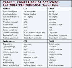
Although CMOS sensors offer some advantages over CCD cameras in specific applications, not all CMOS sensors (much less the cameras) are created equal (see Table 1). "Only a handful of CMOS sensor manufacturers cater to the industrial vision market," says PixeLink's Bisson. "Most are designed for the consumer digital-camera market and can go out of fashion in 12- to 18-month cycles. You want to make sure your sensor is supported for at least three years. FillFactory and Micron Technology are two of the biggest suppliers that promise long-term support. Fabless sensor manufacturers have less ability to guarantee this service," concludes Bisson.
Bisson also recommends that end users be familiar with how the camera manufacturer deals with three major challenges of CMOS technology: fixed-pattern noise (FPN), photoresponse nonuniformity (PRNU), and parasitic sensitivity. CMOS camera manufacturers use flat-field correction, which adjusts the gain and offset control for each pixel to counter FPN and PRNU, both of which should be addressed at the factory.
Sometimes, pixels cannot be corrected and, as such, are identified as defective. Manufacturers typically fix this by replacing the pixel with values from a neighboring pixel, which is less effective, or by using an average or gradient based on neighboring pixels. The more pixel values taken into account, the better the final image, but the more space is required on a nearby FPGA to perform the correction.
Bisson adds that this is less of an issue with larger arrays because a single pixel is not as likely to affect the image quality as the array increases in size. "Some manufacturers publish a map of the defective pixels per sensor," Bisson says, adding that the number of defective pixels is usually less than 0.01% of the total array. Manufacturers should provide a software tool for on-site flat-field correction that takes into account uneven lighting and corrects it.
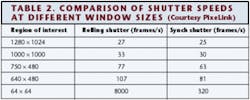
Parasitic sensitivity occurs when a pixel continues to collect charge after shuttering. This is more of a problem with systems installed in locations with excessive ambient light or with systems that do not strobe the light source. CMOS sensors typically use one of two shutter methods: rolling shutters or global shutters. Rolling shutters are faster, reading out one row of pixels while exposing another, but are better suited for step-and-repeat applications rather than high-speed applications because smear can be introduced if the object moves during a shutter cycle (see Table 2).
Global shutters take longer for a full exposure/read cycle because the steps are not combined as they are with rolling shutters. If the read cycle or time between frames is long compared to the exposure time, it increases the level of parasitic noise. Bission says, "You want to make sure that the total charge collected during integration time is at least two orders of magnitude greater than the total charge collected during readout. This is the biggest challenge facing CMOS sensor manufacturers."
A final shutter option is the extended shutter. Extended shutters allow an imaging system to capture usable images of scenes requiring large dynamic ranges, such as in welding and traffic-control applications. Extended shutters are essentially a logarithmic response in which the camera exposes the pixels in dark areas of the field of view for longer than bright areas by effectively resetting the charge for pixels that are saturated by exposure to bright light.
Company Info
Dalsa, Waterloo, ON, Canada www.dalsa.com
FillFactory, Mechelen Belgium www.fillfactory.com
Integrated Design Tools, Tallahassee, FL, USA www.idtvision.com
Micron Technology, Boise, ID, USA www.micron.com
National Instruments, Austin, TX, USA www.ni.com
PixeLink, Ottawa, ON, Canada www.pixelink.com
ShapeGrabber, Ottawa, ON, Canada www.shapegrabber.com
The MathWorks, Natick, MA, USA www.mathworks.com


