Choosing a SWIR Sensor for Machine Vision Applications
Machine vision using short-wave infrared (SWIR) wavelengths can accomplish unique tasks that would be difficult, or even impossible, using conventional imaging systems. For example, SWIR imaging can see through plastic containers that are opaque to visible light to measure their contents (Figure 1). Advances in SWIR camera sensors have significantly reduced their cost in recent years, opening up a new wave of SWIR machine vision applications. However, some of the newest SWIR sensors have prioritized shrinking pixel sizes to maximize resolution, but this has driven the cost of the sensors back up to where it used to be. While SWIR imaging is a powerful tool for extracting information that cannot be obtained through conventional imaging, focusing on SWIR wavelengths introduces new challenges for the optics used in these systems.
This article will dive into these trends in SWIR imaging and how they are shaping the machine vision landscape.
A New Generation of Sensors Has Made SWIR Imaging More Accessible
Recent developments in SWIR imaging sensor manufacturing led to a new generation of affordable sensors covering visible and SWIR wavebands from 0.4 to 1.7 µm. These new sensors also do this with low noise and high quantum efficiency—a term that describes the efficiency of incident light being converted to electric signals. While low noise and high quantum efficiency have been available in sensors designed for visible wavelengths for years, they have not been nearly as available for SWIR wavelengths until more recently.
The traditional sensors for SWIR applications are based on indium gallium arsenide (InGaAs), and they have been used to achieve high performance over SWIR wavelengths for years. However, they are difficult to manufacture and, therefore, expensive. They still achieve the best efficiency and sensitivity of all available SWIR sensor types, but their high manufacturing cost often makes them cost-prohibitive. The newer, more affordable generation of SWIR sensors do not achieve quite as high performance as InGaAs sensors, but their resolution, noise, and efficiency are often more than sufficient for many imaging systems—at a significantly lower cost.
Key Considerations for SWIR Imaging
Knowing which SWIR wavelengths are best for your application, from the beginning, is difficult to determine because our eyes cannot detect SWIR wavelengths. We do not have strong intuition regarding SWIR imaging. When using visible wavelengths, for example, it is typically simple to guess whether a red light source will highlight red components to enhance contrast or if blue illumination will make the background appear darker. When creating a SWIR machine vision system, the system designer often needs to determine the spectral properties of all materials being inspected in advance, as interactions with SWIR light are not as intuitive.
One way to determine the correct SWIR wavelengths needed for an application is to find existing documentation on the material being imaged. Plots of its absorbance or transmittance show which wavelength(s) will appear bright or dark and which will give you the best contrast.
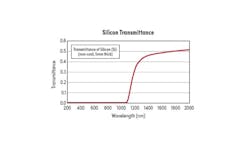
For example, silicon is known to be transparent to SWIR wavelengths longer than 1100 nm (Figure 2). Because of that, SWIR imaging is often used for various types of silicon defect identification including crack detection, bonding inspection, spotting internal defects on the wafers themselves, or detecting defects in circuits formed with different materials on silicon substrates.
A SWIR hyperspectral camera and a broadband illumination source can also be used during the system development phase to figure out the best wavelength(s) to focus on. This captures images covering many different wavelengths, as well as a spectral signature for each pixel. Using this information, the system designer can identify if one or several wavelengths of interest have a strong peak of absorption or transmission that allows the machine vision system to maximize contrast and accomplish its task. An example is shown later in the SWIR Imaging Applications section.
While the hyperspectral camera and broadband light source will likely be expensive, they will identify the key wavelength(s) of interest. Then, when the final system is created in higher volumes, a simpler SWIR camera and illumination source optimized for this specific wavelength are used, resulting in a more cost-effective final system.
When using the hyperspectral light source and camera for product development, sometimes contrast cannot be maximized by using a single wavelength or small group of wavelengths. In those cases, the final system may also need to use more complicated hyperspectral systems. In addition to more expensive cameras and illumination sources, this also increases the complexity and cost of the imaging lenses used. However, this is required in some material sorting applications like plastic recycling, food quality inspection , and foreign material detection.
SWIR Imaging Applications
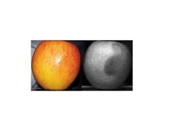
A common application of SWIR in machine vision is identifying moisture (Figure 3). Water has an absorption peak around 1450 nm that appears very dark to a SWIR imaging system. This is useful in many applications like moisture detection in fruit inspection, food processing, bottle fill level inspection, and agricultural applications.
Not all liquids absorb SWIR wavelengths the same way water does, allowing SWIR imaging to easily differentiate liquids that may look identical under visible inspection (Figure 4).
Unique Challenges for SWIR Imaging Lenses
Many imaging lens assemblies designed for use with visible light can also transmit some SWIR radiation, but you can significantly increase the performance of your SWIR system by using lenses designed specifically for this wavelength range. This changes the waveband that the lens design is optimized for, the glass types used to maximize SWIR light throughput, and the coatings applied to the lens elements.
Materials like germanium, silicon, sapphire, and zinc selenide have higher transmission for SWIR wavelengths and can improve SWIR imaging performance, but they are more expensive than the glass types used in conventional imaging lenses.
The Newest SWIR Sensors Are Driving Prices Back Up
The newest SWIR sensors that have entered the market are reversing the trend of making SWIR applications more accessible. They offer smaller pixel sizes than other available sensor types and increase system resolution, but this drives costs back up to where they were before. Not only do they make SWIR cameras more expensive, but they place more demands on the imaging lenses used with them and make those more expensive as well. In order to achieve resolutions high enough to take full advantage of these new sensors, optical designs become more complicated and tolerances are tightened.
The cost of SWIR optics is already high because of the unique materials required. This two-fold increase in SWIR system costs associated with the newest SWIR sensors will likely result in the newest sensors not having as significant an impact on the machine vision landscape as the previous generation of SWIR sensors that made these applications more accessible.
SWIR imaging can accomplish impressive feats unachievable with conventional visible imaging, and the decreased cost of SWIR sensors in recent years has made SWIR imaging more accessible than ever before. But while the smaller pixel sizes of the newest SWIR sensors will benefit the highest-performance SWIR systems, for many, the newest sensors indicate a return to SWIR imaging being cost-prohibitive. Because of this, the newest sensors may be ignored by many machine vision system systems designers and fail to dethrone the previous wave of more affordable SWIR sensors.
About the Author

Cory Boone
Cory Boone is the Technical Marketing Manager at Edmund Optics’ Woodcrest, NJ, USA office. He leads the creation of technical content including application notes, published articles, video scripts, and case studies. He also plans the company’s technical content strategy, coordinates with different business units, and acts as the technical voice of the marketing department. He received a BS in Optical Sciences and Engineering with minors in Math and Material Science Engineering from the University of Arizona and an MBA from the University of North Dakota.

Nicholas Sischka
Nicholas Sischka is the Director of Imaging Product Development at Edmund Optics’ Cherry Hill, NJ, USA office. Specializing in optics for vision systems, Sischka supports imaging and machine vision customers with application knowledge and design assistance for modification or customization requirements. Additionally, Sischka serves as the A3 (Association for Advancing Automation) NextGen Chair and teaches on the A3 Education Committee. He holds a BS in Optical Sciences and Engineering from the University of Arizona.


