High-volume cmos imagers target low-cost applications
High-volume cmos imagers target low-cost applications
Andrew Wilson
Editor at Large
For more than two decades, charge-coupled devices (CCDs) have been the technology of choice for cameras, video cameras, digital still cameras, facsimiles, and copiers. However, CCDs are more complex and expensive to produce than complementary-metal-oxide-semi-conductor (CMOS) based sensors and require multiple power supplies and more support devices.
As a result, semiconductor vendors are trying to harness the volume-manufacturing capability of CMOS fabrication lines to provide low-power, low-cost image-capture sensors. When compared to CCDs, CMOS-based sensors can reduce total system cost, use less power, and incorporate higher levels of integration.
Incorporating on-board analog-to-digital converters, timing chips, and synchronization circuits, single-chip CMOS cameras are available from a number of vendors including Conexant Systems (Newport Beach, CA), Vision (San Jose, CA), and Symagery Microsystems (Kanata, Ontario, Canada). And, because these imagers are manufactured in industry-standard CMOS wafer-fabrication facilities, they can be produced in high volumes, reducing the cost of many imaging applications such as those involved with videoconferencing and digital still cameras.
Low cost, high volume
Structured as low-cost, high-volume devices, CMOS imagers have increasingly attracted attention from suppliers, systems integrators, and users over the past year based on the concept of a "camera on a chip." However, CMOS-based cameras used in industrial applications must deliver low noise and high responsivity under harsh factory conditions. "There`s a lot of hype out there right now on CMOS image sensors," says Savvas Chamberlain, president and chief executive officer of Dalsa Inc. (Waterloo, Ontario, Canada), "not only from the media but unfortunately also from technical people and companies promoting CMOS sensors."
Both CCD and CMOS imagers sense light by converting incident photons into electrons using either a photodiode or a photogate as a sensing element. However, CCDs dedicate maximum pixel area to photon-charge collection and then transfer this charge to an amplifier at the edge of the die. On the other hand, the charge packets collected in CMOS devices are detected by charge-sensing amplifiers fabricated from CMOS transistors within each pixel at the expense of reducing the total optically sensitive area. This information is then read out using an x-y addressing scheme similar to that used in random-access-memory (RAM) devices.
CMOS imagers can be classified as either passive or active. In passive-based CMOS sensors, each photodiode or photogate acts as a sensing element where charge is collected and then read out, often by an array of amplifiers positioned at the top of each column of pixels. "Because raw pixel signals are not buffered or processed on-chip, images are susceptible to signal degradation by parasitic capacitance in the multiplexer structure," says Bart Dierickx, head of the imager development group at IMEC (Leuven, Belgium). "However, this can lead to small pixel sizes or relatively large photosensitive areas," he adds.
To overcome these shortcomings, CMOS sensor suppliers are developing "active-pixel" CMOS sensors where buffers and amplifiers are used to decouple the resulting electronic signals from the photosites. This complex architecture uses local signal conditioning and processing to achieve lower noise but an inferior fill factor (proportion of light sensitive area in each pixel) than that of passive-pixel CMOS devices.
Research sponsored by the NASA Office of Space Access and Technology led to several commercial applications of CMOS imagers under the direction of Eric Fossum, now chief scientist at Photobit (Pasadena, CA). The company has developed a 2/3-in., CMOS-active-pixel digital image sensor that can operate at up to 60 frames/s in progressive-scan mode with a resolution of 1280 x 720 pixels.
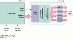
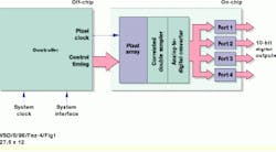
With on-chip 10-bit analog-to-digital converters (ADCs), the device provides a row of analog multiplexers below the pixel array that allows dark-current calibration and ADC testing (see Fig. 1). According to preliminary specifications, the device offers a fill factor of 23% and an internal intrascene dynamic range of 75 dB.
Integrate or not
Both active and passive CMOS sensors can use either nonintegrating or integrating outputs. In an integrating imager, the output signal of any pixel is proportional to the charge collected during exposure time. This charge is accumulated from the photons that impinge on each pixel. Integration starts with the reset or drainage of all charges present in the pixel and ends with charge readout. In between these two functions, the pixels can not be accessed. Therefore, like CCDs, integrating CMOS imagers can be read only under the direction of a strict timing scheme.
In nonintegrating CMOS sensors, the direct readout of a signal is proportional to the photocurrent generated in the pixel`s photodiode or phototransistor. Nonintegrating CMOS devices require no timing mechanism and can be accessed directly or asynchronously like a memory device. Based on this design, direct readout imagers are pixel addressable. Such direct imagers also feature a logarithmic photoelectric transfer curve, resulting in a wide optical dynamic range, compressed into a linearly scaled output signal. "However," says IMEC`s Dierickx, "such sensors produce rather low image quality because of high readout noise and nonuniformity."
In the IMEC Fuga15d, a 512 x 512-pixel three-transistor phototransistor imager, each photodiode is placed in series with a nonlinear resistor. The resulting logarithmic response captures a range of intensities at the same time in the same image. Cameras based on such devices can image outdoor scenes from an inside location and retain the imaging details of both inside and outside scenes (see Fig. 2). With a classic, linearly integrating CCD or CMOS sensor, either the outdoor scene would saturate to white or the indoor scene would be totally black. The Fuga15d can capture six or more orders of magnitude of intensities in the same image. Dalsa has previously offered CCDs with the same dynamic range using a patented photodetector; therefore, logarithmically responsive CCDs can be fabricated.
Due to the large inherent nonuniformity of the Fuga15d, all the pixels must be calibrated to obtain an image with acceptable quality. This calibration is performed by subtracting an offset stored in memory from every pixel readout value. Such offsets are obtained by reading a homogeneous white or gray image with representative brightness levels.
In integrating CMOS imagers, three readout methods are generally adopted. The first method reads a pixel`s signal value after the integration phase. The second method, called double sampling, outputs the difference between the postintegration signal and the subsequent reset level of that pixel. In this way, local signal-path nonuniformities are effectively suppressed. Correlated double sampling, the third method, works like double sampling but uses the difference between the postintegration signal level and its preintegration reset level. Due to this correlation between signal level and reset or reference level, capacitor noise is suppressed. However, correlated double sampling requires the temporary storage (one frame time) of all the reset levels associated with each pixel.
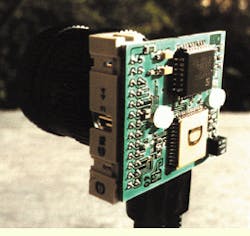
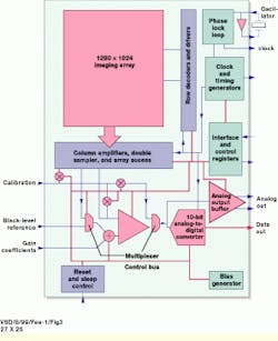
Correlated double sampling can be implemented digitally as an off-sensor RAM or, as represented in the design of the VCA1280 digital video camera IC from Symagery (Kanata, Ontario, Canada), in the pixel itself. Operating as a 1280 x 1024-pixel resolution, 1-in. CMOS image sensor, the device incorporates all of the sensor timing and control, clock generation, video conditioning, and conversion electronics used in a digital camera (see Fig. 3).
To minimize temporal noise and the effects of transistor mismatches, the device uses on-chip double sampling. In addition, it has the capability to independently characterize sources of on-chip fixed pattern noise. Photoresponse nonuniformity is provided through a calibration mode that can be measured through an externally supplied voltage.
Lower cost
Because CMOS-based sensors can be built by conventional semiconductor production lines, they are often touted as a lower-cost alternative to CCDs. When compared to CCDs, such sensors do require less power and can incorporate higher levels of integration. "However," says Alireza Moini of the University of Adelaide (Adelaide, Australia), "such vision ICs are based on the concept that analog VLSI systems with low precision are sufficient for implementing many low-level vision algorithms. In fact, the precision in such analog systems is based on several factors that are uncontrollable," he adds.
Moreover, many advanced processes for high-level integration are usually tuned and characterized for leading-edge DRAMs and processors. In addition, many available processes do not have a specific photodetecting element and are not well tuned for analog circuit design.
Dalsa`s Chamberlain agrees. "To overcome poor fill factors, CMOS imagers typically use nonstandard CMOS processes, such as microlens technology, to focus the light away from the active circuitry onto the photosensitive portion of the pixel," he says.
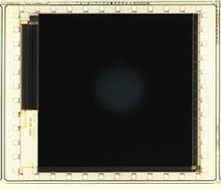
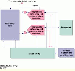
CMOS microlens technology is currently being used by a number of manufacturers, including Conexant Systems. In the design of its CN1024 digital CMOS imager, for example, the company has developed a 1024 x 768-pixel gate-array resolution imager (see Fig. 4). With a 10-bit digital output, this device includes on-chip suppression of reset noise, spatial noise suppression using black frame subtraction, and on-chip correlated double sampling.
Developed using microlens technology, this design results in a 25% drawn fill factor, according to preliminary information from Conexant. When compared to the high fill factors of CCD devices, CMOS sensors are performance limited. The Dalsa IA-D4 progressive-scan CCD area sensor, for example, offers 1024 x 1024-pixel resolution at 40 frames/s and a 100% fill factor while achieving high-speed, low-light imaging.
Portability and scalability
"With submicron CMOS design rules especially, there is no such thing as portability or scalability with imaging photosites if any level of performance is to be maintained. If there is a foundry process change or if the design is ported to another foundry, the pixel design will have to be reoptimized," says Dalsa`s Chamberlain.
Because of these limitations, Dalsa does not, at present, compete in the low-performance, high-volume, CCD image-sensor market. "If we did," notes Chamberlain, "we would be competing against large multi-national companies such as Intel Corp. (Santa Clara, CA), Motorola Semiconductor (Austin, TX), and Mitsubishi Electronics America (Sunnyvale, CA).
For high-performance, premium-price vision applications, Chamberlain has, however, alluded to company plans to develop CCD linear arrays for applications that do not have the problem of on-chip amplifiers taking up active imaging area. "Essentially," he says, "applications that are neither light-starved nor photon-limited and can use on-chip signal processing are candidates."
FIGURE 1. Incorporating an active photodiode pixel array and associated analog-to-digital converters, the Photobit PB-0720 CMOS image sensor can be used with the company`s field-programmable-gate-array-based controller to produce 1280 x 720-pixel resolution images.
FIGURE 2. Direct imagers feature a logarithmically compressing photoelectric transfer curve, resulting in a wide optical dynamic range. The resulting logarithmic response allows a range of intensities to be captured at the same time in the same image. This capability allows cameras (top) based on devices such as the 512 x 512 Fuga15d from IMEC (bottom) to image outdoor scenes from an inside location, while retaining the imaging details of both inside and outside scenes.
FIGURE 3. To minimize temporal noise and the effects of transistor mismatch, the 1280 x 1024-pixel VCA1280 imager from Symagery uses on-chip double sampling. A calibration mode can be used to characterize sources of on-chip fixed pattern noise and photoresponse nonuniformity.
FIGURE 4. To overcome fill-factor limitations, CMOS imagers such as the Conexant CN1024C use a nonstandard CMOS process called microlens technology to focus the light away from the active circuitry and onto the photosensitive portion of the pixel. This process results in a 25% drawn fill factor, compared to fill factors as high as 100% in CCD devices, such as the Dalsa 1024 x 1024-pixel IA-D4 progressive-scan sensor.
Company Information
Conexant Systems
Newport Beach, CA 92658
(949) 483-4600
Fax: (949) 483-4078
Web: www.conexant.com
Dalsa Inc.
Waterloo, Ontario, Canada N2V 2E9
(519) 886-6000
Fax: (519) 886-8023
Web: www.DALSA.com
IMEC
B-3001 Leuven, Belgium
+32 (0)16 28 12 66
Fax: +32 (0)16 28 15 01
E-mail: [email protected]
Web: www.imec.be/ms/mst/Welcome.html
Intel Corp.
Santa Clara, CA 95052
(408) 765-8080
Fax: (408) 765-9904
Web: www.intel.com/pressroom/archive/ releases/pi092898.htm
Mitsubishi Electronics America
Sunnyvale, CA 94086
(408) 730-5900
Fax: (408) 732-9382
Web: www.mitsubishichips.com/products/ assps/a_retina/index.htm
Motorola Inc.
Austin, TX 78721
Web: mot-sps.com/ADC/Image_Capture/
Photobit
Pasadena, CA 91101
(626) 683-2200
Fax: (626) 683-2220
Web: www.photobit.com/
Symagery Microsystems
Kanata, Ontario, Canada K2K 2X2
(613) 599-6500
Fax: (613) 599-6501
E-mail: [email protected]
Web: www.symagery.com/
Vision
San Jose, CA 95129
(408) 556-1550
Web: www.vvl.co.uk/
