Waveguide fab adds microscopy to vision
By Lawrence J. Curran, Contributing Editor
A novel optical microscopy and vision system from Optical CrossLinks (Kennett Square, PA) serves as its core of laser micromachining operations for manufacturing polymer waveguides. Use of the microscopy/vision system enables the company to locate and measure waveguides more precisely than with previous methods. This system also enables the company to bring prototype and batch processing of components in house, resulting in a substantial reduction in the processing time previously required by an outside source. The company designs, develops, and fabricates both passive and active planar optical waveguides in flexible polymer sheets.
The waveguides serve as optical components that are used in chip-to-chip communications via optical fiber, as in transmitting signals from a switch to a microprocessor, for example. They are fabricated in a flexible acrylate-type polymer film for use in a variety of products that operate from 600 to 1650 nm.
Jim Hohman, vice president for engineering, says that the polymer system allows for passive alignment of optical fiber to waveguide with low coupling losses. This approach also provides an easy path to make slot connectors for quick connection of motherboard-to-daughterboard configurations. The waveguides can be laminated to silicon wafers and other materials. Multiple layers can also be laminated together to create multi-layer optical circuits and circuit boards. The process also provides a method to embed active and passive components such as photodetectors, filters, and lasers.
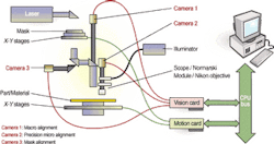
NanoVia LP (Londonderry, NH) supplies the optical/machine-vision system used in both prototyping and batch-scale production by Optical CrossLinks (see Fig. 1). Todd Lizotte, NanoVia's vice president for research and development, says his company had provided previous systems to Optical CrossLinks.
null
Challenging problems
There were several design challenges in the current application. According to Lizotte, Optical CrossLinks needed a machine-vision system to acquire images of 6-µm-wide, single-mode, polymer waveguides within a sheet of bulk material. The contrast difference between the waveguides and the bulk material was <0.03%.
After the waveguides are created in the film, they must be precisely located for subsequent processing steps, which might include the insertion of active and passive components. "The waveguide has to be acquired using a computer-vision system that clearly views the waveguide center and determines a centroid [in the material] to within ±0.50 µm," Lizotte says.
Hohman explains that the film begins as a monomer inside a polymer base. The polymer sheets are 50 to 250 µm thick and as large as the photomask used, which can be 13 × 16 in. Optical CrossLinks offloads the film from a roll, performs step-and-repeat operations on it, and exposes the film to light from an ultraviolet (UV) lamp through the mask, polymerizing the film to create waveguides at the exposed points. "The UV floodlight locks those points with a high material density, creating waveguides that keep light from propagating through those points," Hohman says. The operation is similar in principle to semiconductor step-and-repeat lithography that transfers circuit features to a wafer.
Before those steps could be reached in the NanoVia-Optical CrossLinks collaboration, hardware and software had to be developed that could deliver the precision needed to pinpoint the waveguides in the material so that they can be aligned and measured by the vision system. The innovation aspects included the optical microscopy and vision system developed by NanoVia and the application software written by Optical CrossLinks.
Camera assistance
NanoVia's Lizotte points out that the vision system delivers high accuracy as long as the microscopy optics can resolve an image and the camera's pixel resolution can achieve the required precision. "When trying to measure and align single-mode polymer waveguides, however, difficulties arise because of the slight contrast differences between the waveguides and the bulk material," he explains.
Furthermore, the bulk material is translucent, being built up using several laminate levels that can cause undesirable illumination when exposed to transmitted light. "Because we needed an alignment tolerance of ±0.50 µm, several techniques had to be integrated to form an optimum optical scope system," adds Lizotte.
NanoVia used differential interference contrast (DIC) microscopy to improve the contrast in images. "We found that a modified Nomarski DIC technique using coaxial incident light illumination was the best approach for this application," Lizotte says. In a Nomarski-modified Wollaston prism, the crystals are cut obliquely to the optical axis; this allows the "plane of fringe localization" to be outside the prism, and, therefore, in the back focal plane of the objective. This allows the combining prism to be placed in the objective turret, simplifying the setup for Nomarski DIC.
In conjunction with the DIC technique, an oblique holographic illuminator using monochromatic high-intensity light-emitting diodes (LEDs) assists the main DIC microscopy. The oblique technique also supports alignment and secondary process steps in which more macrofeatures need to be viewed in relation to the microfeatures being viewed by the DIC system. "In the Optical CrossLinks application, the task was to integrate all these attributes into a single scope to perform repeatable and accurate alignments and measurements," Lizotte explains.
In coming up with this design solution, he says, the first thing to determine is the camera resolution required to achieve the customer's precision level. "Because the design goal is ±0.50 µm, we can determine that the required microns/pixel ratio is approximately one-fourth of the target tolerance. Using a 1/3-in., 640 × 480-pixel camera chip, the field of view becomes approximately 76 × 58 µm on the target," Lizotte adds.
Scope optics
Based on these calculations, NanoVia chose an objective lens with a high numerical aperture and a good working distance. "An infinity-corrected 20X objective lens from Nikon Instruments (Melville, NY) with a 0.35 numerical aperture and a 20.5-mm working distance turned out to be the best choice for this application," Lizotte says. Next, NanoVia built a custom adjustable-wedge prism assembly to tune in a phase difference of up to 0.7 wavelength—the separation between the object and reference beams.
The assembly also includes an analyzer and polarizer elements mounted on an insert slide located on the coaxial illuminator port. The two elements are fixed at a point where the object beam and the reference beam are balanced in intensity. Each of these elements is integrated into a Thales Optem (Fairport, NY) Zoom scope tube system. Surrounding the tube assembly is a ring illuminator of LEDs with a ring of computer-generated diffractive optical elements (CGDOE) placed onto the LED ring so that each CGDOE element is centered on each LED illuminator.
Each CGDOE element shapes and vectors the light to illuminate the field of view of the microscopy system. This ring illuminator ensures 360° illumination over the objective's field of view with overlapping beams of shaped light providing an integrated homogenous zone of light. The combination of oblique and incident illuminations from the microscopy system ensures maximum contrast and minimizes adverse shadowing effects. Matched with a high numerical aperture objective, the machine-vision software performs accurate measurements and alignments on the images being observed and acquired by a frame grabber.
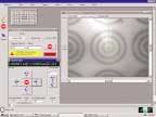
Lizotte concludes that, using oblique illumination alone, the camera system shows only minor details, but not with sufficient contrast to achieve the required alignment precision. "With the addition of the modified DIC module, however, the resulting image has crisp contrast and resolution ready for precise machine vision analysis" (see Fig. 2).
null
System structure
The key components of the NanoVia vision system used by Optical CrossLinks encompass three CCD cameras, a scope-optics module, vision software, frame grabber, motion software, motion controller, two illuminators, various stepper and servo motors, and x, y, z motion stages. Lizotte says the system controller uses a Windows-based operating system (OS), developed by NanoVia in Visual C and Visual Basic programming languages. The OS runs on a Pentium 4-based PC and links the motion, vision, and laser-processing functions. The motion software is NanoVia's NV3 application package, which was codeveloped with Axis New England (Woburn, MA).
The CCD cameras are RS-170, 1/2-in., CCD video models from Sony Electronics (Park Ridge, NJ). The frame grabbers are supplied by Data Translation (Marlboro, MA), which also furnishes its Vision Foundry vision software.
The scope optics were integrated by NanoVia and comprise a Thales Optem Zoom 100C microscope and a 20X external objective holder and a 20X internal objective holder from Nikon Instruments. One illuminator is NanoVia's IllumiCAM; the second is an EKE 150-W unit from Schott-Fostec (Auburn, NY). Delta Tau Data Systems (Chatsworth, CA) provided its PMAC2 motion-control card.
System operation
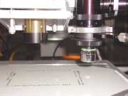
During system operation, an adhesive holds the polymer sheets in place on a glass plate. The waveguides, as well as the fiducials used to align the polymer sheet, have already been formed by the UV lamp. The glass plate, in turn, is held in place under the optics by a vacuum chuck. Camera 1 performs the macro-alignment for accurately aiming the laser beam after camera 3 has properly aligned the photomask.
Camera 2, which is the IllumiCAM, precisely locates the fiducials and waveguide (see Fig. 3). The vision system software initially finds the centroid of the waveguide; then, the laser cuts a slot to terminate the waveguide. Lizotte explains that the cuts need to be made exactly on center so that the optical fiber that will be attached to them aligns to the center of the waveguide, or to assure that the waveguide is precisely aligned for whatever subsequent processing the waveguide design requires. This might include the insertion of other components.
null
Lizotte says locating the waveguide presented the most difficult challenge the system had to meet. "The waveguide is transparent, as is the bulk material in which it is fabricated," he stresses, "and the contrast difference between them is less than 0.03%. Using a pseudo-3-D approach, the IllumiCAM allows us to see the waveguide even though it is embedded in the bulk material."
Optical CrossLinks' Hohman says his company added the fixture and the vacuum chuck to hold the polymer sheets in place under the integrated system NanoVia supplied. Optical CrossLinks also wrote software to control the system, which was in production within a month after its installation.
Company Information
Axis New England
Woburn, MA, USA
www.axisne.com
Data Translation
Marlboro, MA, USA
www.datx.com
Delta Tau Data Systems
Chatsworth, CA, USA
www.deltatau.com
NanoVia LP
Londonderry, NH, USA
www.nanovia.com
Nikon Instruments
Melville, NY, USA
www.nikonusa.com
Optical CrossLinks
Kennett Square, PA, USA
www.opticalcrosslinks.com
Schott-Fostec LLC
Auburn, NY, USA
www.schott-fostec.com
Sony Electronics Inc.
Park Ridge, NJ, USA
www.sony.com/videocameras
Thales Optem
Fairport, NY, USA
www.thales-optem.com


